Beyond gaming, the graphic card is useful in Edge AI applications, leveraging OpenVino for streamlined AI development and deep learning integration.
ADLINK Technology Inc. unveils its latest innovation, the EGX-PCIE-A380E graphics card, marking its debut in the realm of low profile PCIe form factor graphics cards. Embracing the formidable Intel Arc A380E GPU, this pioneering offering targets the thriving commercial gaming sector, encompassing slot machines, video lottery terminals, and electronic games. Seamlessly integrable into the company’s gaming platforms like the ADi-SA6X, which harnesses the prowess of Intel Core processors, the A380E promises unparalleled platform performance.
Crafted for industrial application, it has an exceptional cost-to-performance ratio, coupled with high reliability and minimal power consumption, capped at a mere 50W. Upholding the company’s hallmark commitment to longevity, this industrial-grade marvel assures availability for a minimum of five years. Its slender, single-slot design, measuring a mere 69mm x 156mm, underscores its compactness and versatility.
While its primary domain lies within commercial gaming, the card transcends boundaries, finding relevance in diverse industrial edge AI applications like Industrial IoT and retail analytics. From powering video walls to facilitating media processing and delivery, its utility spans myriad sectors.
Aligned with the OpenVino open-source toolkit, the A380E streamlines AI development and deep learning integration, particularly in computer vision domains. Moreover, it boasts compatibility with DirectX 12, Vulkan 1.3, OpenGL 4.6, OpenCL 3.0, Windows 11, and Linux, ensuring seamless operability across platforms. This latest addition enriches the company’s extensive lineup of A350E/A370E MXM GPU solutions, which harness potent Intel Arc discrete graphics. These modules elevate responsiveness, precision, and reliability, catering to time-sensitive edge applications across healthcare, media processing, transportation, and, of course, commercial gaming.
This technical article discusses twelve different methods for laying high voltage cables. Out of the ten, four are deemed conventional and eight are deemed progressive. Many various utilities and companies... Read more
The post Twelve high voltage cable construction techniques used worldwide appeared first on EEP - Electrical Engineering Portal. Credit: EEP- Electrical Engineering Portal. Visit:
This technical article discusses twelve different methods for laying high voltage cables. Out of the ten, four are deemed conventional and eight are deemed progressive. Many various utilities and companies... Read more
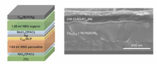
This method achieves good results by suppressing phase segregation with a novel pseudo-triple-halide alloy, paving the way for durable and high-efficiency photovoltaics in the quest for sustainable energy solutions.
In the quest for efficient and affordable solar energy solutions, researchers have focused on organic solar cells utilizing perovskite materials. Compared to traditional silicon-based cells, these organic counterparts offer cost advantages, flexibility, and tunability. Despite achieving a certified power conversion efficiency (PCE) of 19.4%, lower than silicon cells, they hold promise for widespread deployment.
Researchers at Soochow University’s Suzhou Key Laboratory of Novel Semiconductor-optoelectronic Materials and Devices propose a breakthrough strategy to enhance the efficiency and stability of perovskite/organic tandem solar cells. Published in Nature Energy, their method addresses a critical issue known as phase segregation, which hampers the performance of wide-bandgap perovskite cells.
The team successfully suppressed phase segregation by introducing a pseudo-triple-halide alloy into mixed halide perovskites, incorporating iodine, bromine, and pseudo-halogen thiocyanate (SCN) ions. This innovation prevents halide elements from separating within the solar cells, improving crystallization and reducing grain boundaries.
The addition of SCN ions slows crystallization, preventing ion migration and facilitating electric charge movement within the solar cell. These ions enter the perovskite lattice, forming an alloy and occupying iodine vacancies, thereby blocking halide ion migration through steric hindrance.
The researchers achieved good results by testing their strategy on perovskite/organic tandem solar cells. The tandem cells exhibited a PCE of 25.82%, a certified PCE of 25.06%, and operational stability lasting 1,000 hours. This success underscores the potential of their methodology to advance the development of stable, high-efficiency perovskite/organic photovoltaics.
Looking ahead, the team claims that their research could be adapted to various wide-bandgap perovskite compositions, further enhancing the performance and longevity of solar cells. Ultimately, these advancements may lead to the realization of durable photovoltaic systems operating efficiently under diverse lighting conditions, heralding a new era of sustainable energy generation.
Develops the logic design, register transfer level (RTL) coding, and simulation for an IP required to generate cell libraries, functional units, IP blocks, and subsystems for integration in full chip designs. Participates in the definition of architecture and microarchitecture features of the block being designed.
Applies various strategies, tools, and methods to write RTL and optimize logic to qualify the design to meet power, performance, area, and timing goals as well as design integrity for physical implementation.
Reviews the verification plan and implementation to ensure design features are verified correctly and resolves and implements corrective measures for failing RTL tests to ensure correctness of features.
Supports SoC customers to ensure high-quality integration and verification of the IP block. Drives quality assurance compliance for smooth IP-SoC handoff.
Configuration/troubleshooting of Historian, AMS and Advance Algorithms
Perform third party communication e.g. ELC, SLC, Profi bus, SCADA & OPC etc.
Excellent knowledge on Power Plant Technology (Thermal, Combined Cycle)
Exposure on Closed Loop Tuning in Thermal Power Plant
Additional Responsibilities:
Lead site activities independently, if required
Participation in meetings with customer and front offices
Prepare daily / weekly reports and MOM as required.
Project Engineering
Design/Implementation of controls from SAMA /Functional diagrams.
Implementation of graphics from sketches/snapshots
Creation/modification of Ovation Internal Point Database
Implementation of Simulation logics for First-Pass Test
Virtual controller setup for testing purpose
Testing of implemented controls and graphics& troubleshooting while testing.
Follow Department Quality processes and procedures.
Scaling of Open loops & closed loops as per the ranges in the HW database
Use various Productivity tools such as DBID tool, Audit Tool, Database Productivity Tool, etc.
Conversion of controls and graphics of Third Party DCS/PLC systems to Ovation
Third Party Communication
Support Factory Acceptance Test (FAT) activities!
In-house Ovation Server/ Workstation loading
Who You Are:
You pursue everything with energy, drive and the need to finish. You deliver messages in a clear, compelling, and concise manner and actively listens and checks for understanding. You lay out a detailed schedule and steps for achieving objectives and use landmarks to track and handle the progress of the work.
For This Role, You Will Need
4 years bachelor’s degree / Master’s Degree in ECE, EEE, I&C, E&I.
Proven experience of 2 to 5 years of in Power Plant process, project engineering and commissioning
Preferred Qualifications that Set You Apart:
Excellent written and verbal communication skills.
Problem-solving, decision-making, and planning skills.
Ability to write reports, business correspondence and commissioning documents.
Ability to optimally present information and respond to queries from management, clients and customers.
Accountable for specification, design and verification of mixed-signal and RF chains/blocks including power amplifiers, line drivers, low noise amplifiers, transmit and receive mixers, frequency synthesizer, base-band amplifiers and filters, voltage regulators and band-gap circuits, phase-locked loops (PLLs) and delayed-lock loops (DLLs), data converters (DACs/ADCs), and switched-capacitor circuits. Work closely with digital and system engineers to optimize the system.
Education, Experience & Skills
Master’s/Bachelor’s Degree in engineering from a reputable college. 1 – 8 years of experience in analog transistor-level design in deep sub-micron CMOS. Knowledge of integrated mixed-signal circuits, RF system and architecture is desired. Should take complete ownership of IPs from specification derivation till production. Experience in SPICE and MATLAB simulations is a must. Familiarity with digital signal processing and ESD protection techniques is a plus.
Qualification: BTech/MTech in EEE/ECE/IT/TC/Power electronics
Expertise in System architecture, inverter/converter topologies, complete knowhow of printed circuit boards, thermal management and product enclosures and interactions.
Experience of modeling, development and testing of power electronics systems, including the development of test and validation plans
Experience in developing the Products complying to various industry standards and regulations in aerospace/ medical/ defense/ automotive/ consumer/ industrial domain.
Experience with various power conversion topologies, DC/DC, PFC Converters, DC/AC Inverters , Motor Control, high-voltage/high-power converters, Micro-controllers & Peripherals HW, Digital System, Analog Electronics Design, Magnetics Design (High Frequency Inductors/Switched Mode Flyback/Forward Transformers)
Responsible for requirements capture, high level product conception, product specifications based on requirements received from the customer.
Guiding the design and testing team in designing, simulating and testing the power electronics, analog and digital electronics circuits and analyzing the outcomes to take further decisions or make conclusions
Responsible for design improvisation and optimization for performance, cost and manufacturability
Responsible for drafting reports, reviewing work schedules, maintain work system logs etc.
Providing deliverable such as: complete Bill-of-Materials, block-diagrams, schematics, PCB design documentation, specifications, test data results, and other necessary documentation (HRD, HDD, ATP, DVTP, RCA, WBS)
Prepare technical presentations, proposals
Excellent technical engineering knowledge coupled with solid people leadership skills.
Oversee product development, manage project delivery in an organized, timely and efficient manner
Manage feasibility studies and technical analysis to support new products
This is a full-time on-site role for an Electronics Engineer at Iota International located in Rohtak. The Electronics Engineer will be responsible for day-to-day tasks such as circuit design, electronic testing, and electrical engineering. They will also be involved in electronic engineering and other related tasks.
Qualifications
Electronic Engineering and Electrical Engineering skills
Circuit Design and Electronics skills
Experience in testing electronic devices
Problem-solving and troubleshooting skills
Attention to detail and ability to work with precision
Strong analytical and mathematical skills
Knowledge of industry standards and regulations
Bachelor’s degree in Electronics Engineering or related field
Job Description of Hardware Engineer II FIRE India
The future is what you make it.
When you join Honeywell, you become a member of our global team of thinkers, innovators, dreamers, and doers who make the things that make the future. That means changing the way we fly, fueling jets in an eco-friendly way, keeping buildings smart and safe and even making it possible to breathe on Mars. Working at Honeywell isn’t just about developing cool things. That’s why our employees enjoy access to dynamic career opportunities across different fields and industries.
Honeywell’s Value Engineering (VE) and Component Engineering (CE) Center of Excellence (COE) is a dynamic collective of professionals dedicated to refining product development through innovative engineering and strategic component selection. Working in tandem with GBE’s Engineering and Procurement teams, the VE/CE COE is a global entity tasked with the critical mission of enhancing product margins and driving productivity, thereby securing Honeywell’s competitive edge in the global market. Our mandate spans across all Strategic Business Groups (SBGs), with the exception of AERO, ensuring that value engineering and component engineering principles are consistently applied to deliver tangible savings and superior products. As a hub of flexibility and rapid adaptation, the VE/CE COE is Honeywell’s strategic response to the “ever-evolving” marketplace demands.
Responsibilities
This position provides an exciting opportunity to advance your Engineering and Engineering Services career within one of the Honeywell’s most profitable and dynamic Business units. This Hardware Engineer role is responsible for driving and supporting projects that focuses on product life cycle management to include obsolescence, cost reductions, and design for supply chain resiliency actions. The position is in Honeywell’s HBT portfolio for commercial life and safety systems to include products such as Fire alarm panels, detectors, voice alarm systems etc. The role requires an entrepreneurial approach to apply mechanical design expertise in a global environment while coordinating with cross functional team in design centers, sourcing, manufacturing, quality, and regulatory teams to generate and implement cost saving. This role includes identification of product cost savings opportunities through alternate supplier qualification, product design standardization, and factory transfers.
Key Responsibilities:
Prepare Test Plans for the project to make sure the alternative component will satisfy all requirements and final product performance meets the specification.
Review the current electronic board design considering the current technologies in terms of component, materials & process, propose ideations to reduce BoM cost by redesign & optimization.
Perform Component and Product level Qualification – Provide change description, develop test instructions, and create user guides and manuals.
Conduct redesign activities of an existing product to gain more domain knowledge about Fire Business and understand how to implement the FIRE standards requirements with help of both regulatory team and more experienced R&D colleagues.
Perform a key role in Obsolescence / Shortage issues.
Track record of the design and test (developer test, functional test, automated test, climatic test) using HON specific tools (JIRA, JAMA, etc.).
Design for Manufacturing and Testability
Select component/materials and deal with appropriate component selection tools (Preferred Parts List, Preferred Suppliers List, etc.).
Build and test prototypes, identify issues, and follow up on corrective actions.
Develop test plans and strategies, specify instrumentation, write test procedures, and analyze test results.
Required Qualifications
Bachelor Degree in Electronic Engineering or equivalent subject
Minimum of 5 years’ experience in engineering position, designing electronic products
Knowledge of Value Analysis/Value Engineering principles and techniques
Knowledge of electronic components, their parameters and characteristics and experience with conditional qualification testing
Knowledge of electronic circuits and subsystems.
Knowledge of PCB CAD design systems, CAD tools, and Simulation Tools
Experience in EMC and product testing
Very good written and spoken English, very good communication and negotiation skills, experience multitasking and prioritizing workload.
We Value
Experience in Engineering Testing
Experience with UL/CSA/CE standards, statistical methods and tools, MS Office
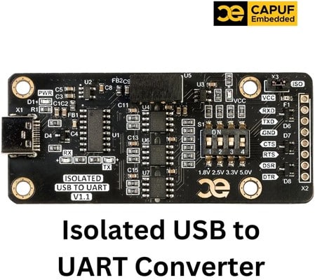
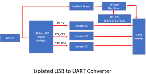
In embedded systems, UART/serial ports are mainly used to view debug messages, to flash the program or to configure the device via command/response protocol.
The Industrial Grade Isolated USB to UART could be useful in various use cases.
High Voltage AC / DC Circuits
Isolated USB to UART Converter is mainly helpful for companies/engineers involved in building power electronics products or dealing with high-voltage DC or AC signals on their boards and want to connect them to a Laptop or PC safely.
Connecting the board with HV AC or DC to a Laptop or PC USB port without isolation may damage the port or laptop. Non-isolated USB to UART converters also induce leakage currents in many situations and can significantly increase noise.
Low Power Embedded Designs which needs 2.5V/1.8V
If you are working on Low-Power Designs like battery-powered asset trackers, wearables, or any battery-powered device, where UART is at a lower voltage level, you will need a USB-to-UART converter that supports those voltage levels.
That’s why CAPUF Embedded’s Isolated USB to UART Converter will help as a voltage section(1.8/2.5/3.3/5.0V) is provided.
Medical Electronics / Noise Sensitive circuits
As safety/induced noise is a great concern in many designs, an isolated USB to UART converter provides the best solution to connect your Embedded Board or product safely with a Laptop or PC.
What is Unique about our Isolated USB to UART Converter?
The board is designed and manufactured in India.
A 4-channel DIP Switch is provided for an easy voltage level selection (1.8V/2.5V/3.3V/5.0V).
Not just RX and TX but RTS, CTS, DSR, and DTR are also provided.
The board can supply ~100mA of power. This power-sourcing capability helps make the setup easy when testing a board that doesn’t need much power.
It provides Galvanic Isolation. Both Power and IOs are Isolated.
Salient Features
USB-C Port: To connect to a PC, one can use a USB-A to USB-C cable or even a USB-C to USB-C cable.
USB to UART Bridge capable of up to 3Mbps
Isolated Power, capable of up to 100mA. Short Circuit Protected.
Isolated RX, TX, RTS, CTS, DTR, DSR, and all IOs are ESD-protected.
Signal voltage level selection 1.8/2.5/3.3/5V via DIP Switch
A 2-pin Jumper is provided to select if you want to power the target(Jumper ON) or if it will be self-powered.
LED Indication for RX, TX, & Power
A male 8-pin header (angled) comes in the package but is unsoldered.
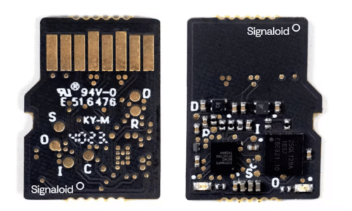
The FPGA development board fits into a microSD slot for easy programming, suitable for wearables, IoT, and predictive modeling.
The Signaloid C0-microSD from Cambridge-based Signaloid is a compact iCE40 FPGA development board designed to fit and be programmed directly through a standard microSD card socket. The core technology is currently offered as an FPGA image for the Lattice iCE40UP5K FPGAs, which are used in the development board.
The tiny FPGA development board is designed for engineers, developers, and researchers involved in FPGA development, edge computing, uncertainty analysis, and embedded systems. Its compact size and unique programming model make it suitable for applications in wearables, IoT devices, and predictive modeling.
The development board features an FPGA, 128 Mbit of flash memory, 11 I/O signals, and two LEDs, all within the footprint of a microSD card. The LEDs are positioned near the top edge of the board, remaining visible when the board is inserted into a socket. Of the I/O pins, six are linked to the microSD interface, while the remaining five are accessible via surface mount pads on the board’s rear.
By inserting the C0-microSD into a host computer, it functions as a file-based device. Applications can communicate directly with the board or utilize the Operating System’s disk utilities. For instance, you can upload a new bitstream directly without needing an external programmer.
Users can also leverage the included Signaloid C0 RISC-V processor core with pre-built uncertainty algorithms for application integration. As the device operates as a microSD card, it is compatible with single-board computers or microcontrollers equipped with an SPI interface.
For further development, the company provides an accessory called the Signaloid SD-Dev carrier board. Measuring 57 x 57 millimeters, this board features a full-size micro-SD card socket, USB-C ports, micro HDMI, and additional connectors, facilitating expanded development and testing.
A Mini Fridge that can work with any power bank and without using harmful CFC gases.
Ever heard of a 5V portable freezer? Yes, you heard it right. In this DIY we design a 5V portable freezer that is easy to carry even while traveling.
A freezer/refrigerator/fridge work on the same principle i.e. Pumping heat from one system to another and thermally isolating both the systems so that the pumped heat from one system cools down.
Meanwhile, the other system keeps getting hotter. The system generally acts like a radiator and transfers heat to a sink which is often the environment. Hence the heat transfer from the target system to the environment is done.
The same principle is used to make the 5V portable freezer. The heat is pumped using a thermoelectric generator. This can generate electricity based on the heat difference or it can pump the heat from one side to another side.
While out on picnics or outdoor activities, having a cold drink is what everyone wishes for especially on a hot day, and hence we wish to have some cold storage or a mini fridge. Since these are only found in luxury cars and vanity vans, and apart from being expensive, the CFC gas is quite dangerous to our environment, especially the ozone layer.
This freezer does not use a CFC gas system that causes harm. Also, it is portable and can operate even with less power. It can run on our phone’s power bank and battery. We can attach it to any car or bus to enjoy chilled drinks, ice cream, etc. on ours.
The freezer is portable and can be carried in a travel bag and set against the car dashboard. It works on a 5V-1.5A power source, like a power bank/battery/solar panel.
Bill of Material
Want to create your own Power Bank? Watch the complete video tutorial for Constructing a Power bank.
Designing Mini Fridge
The body of the freezer has to be thermally isolated as much as possible, hence that is designed first. Thermal isolation is much needed since any freezer works on the heat transfer principle, where heat is transferred from one system to another, making a part of the system much colder.
Since the heat is pumped to another system, it makes the temperature of the recipient increase, so if the thermal isolation is not good, heat continues to enter the system and it becomes hard to maintain the temperature inside the freezer.
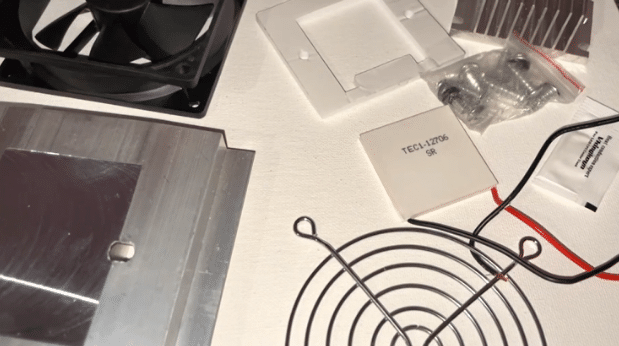
Here we use the PLA 3D printed design of the freezer case and isolate it with thermal isolating material like Polystyrene/thermal isolator spray and paint. For the body of the freezer, one side of the box is kept open while the other 3 are closed. The open side is for inserting the heatsink and thermoelectric cooler module.
Fig 1. Mini Fridge bodyFig 2. Mini Fridge top part
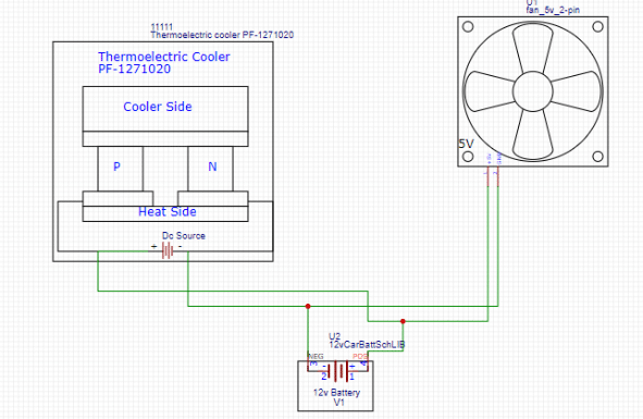
Mini Refrigerator Circuit Connections
The components are connected according to the circuit diagram. The red wire is connected as a +ve wire of the thermoelectric cooler and fan with a 12V power source (battery). The -ve wire is connected with the -ve terminal of the battery and to the -ve wire of the thermoelectric cooler and 12V fan.
The next step is to fix the 3D printed parts and cover the edges with thermal insulator spray foam. Then the door of the freezer is added. A same-size transparent acrylic sheet is cut out and then fixed, such that using a magnetic-based lock system, we can use the door for opening and closing. Magnets are also fixed, on the door and fridge on the body as in Fig 6.
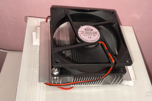
Fig 3 . Thermoelectric TEC Peltier connection for mini fridgeFig 4. Components used for designing a mini-fridgeFig 5. Mini Fridge in ActionFig 6. Attached magnet within the mini fridge
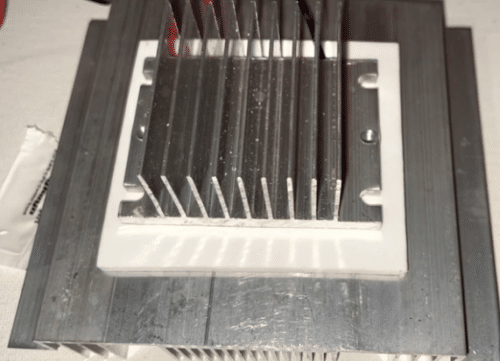
The heatsink and fan are fixed, after which the thermal paste is added and sandwiched between the thermoelectric cooler module and the heatsinks. The fan is added next to the top of the big heat sink fan as in shown in the figures below. (Refer Fig. 7, 8, 9, 10, 11, 12).
Fig 7Fig 8.The thermal paste on a heat sink Fig 9. Thermoelectric fixed and sandwiched between the heatsinkFig 10. Fan added to heatsink fin
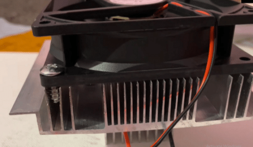
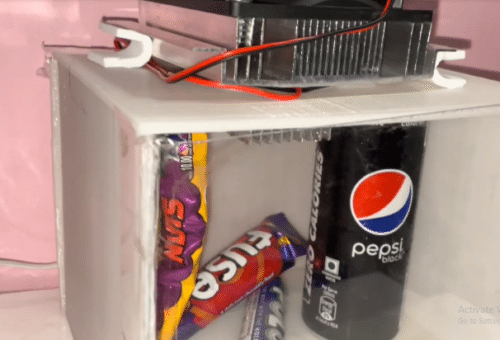
Now the heatsink fan is fixed on the top of the refrigerator while inserting the smaller heat sink inside the refrigerator case. Warm the cut part of the refrigerator body and keep the fan exposed on the other side of the refrigerator. (Refer Fig 13,14,15,16).
Fig 11. The fin fixed on the top part of the refrigerator bodyFig 12. The small heatsink fin fixed inside the refrigerator bodyFig 13. Fan exposed to openFig 14. Refrigerator ready after fixing components.
Now power the freezer, which means the fan and thermoelectric cooler will now wait for a few minutes. The heat is now transferred from the inside of the freezer to the outside, making the inside cooler. After 15 minutes the freezer temperature goes down to around 0 degrees Centigrade, making it ready to use.
Your portable freezer is now ready to use and chilled water, ice, beer, and cool drinks can be stored. It can also be carried around anywhere you go, be it for picnics, outings, hiking or can be fixed in the car.
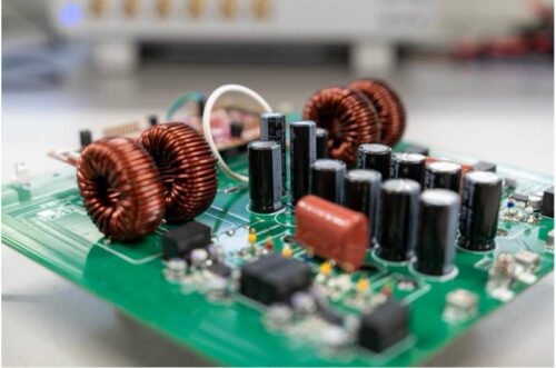
This reference design not only fulfills a variety of functional requirements but also underscores the adaptability and efficiency of using advanced MOSFET technology in conjunction with a dedicated controller for automotive power systems.
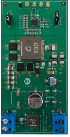
The reference design TND6290/D by onesemi provides a detailed, functional example of how the NCV881930 controller can be effectively utilized in developing a high-performance automotive pre-regulator. The design is not only a testament to the capabilities of the controller but also serves as a reliable blueprint for designers looking to implement a similar solution in their automotive systems. T
This reference design of a 100 W non-isolated synchronous buck automotive pre-regulator is built using the NCV881930 synchronous buck controller, complemented by four NVMFS5C460NL 40 V N-channel MOSFETs, to deliver robust and efficient power management suitable for a wide range of automotive applications. These features include integrated compensation which simplifies circuit complexity, a low quiescent current that enhances battery life, and a continuous synchronous mode for better efficiency under varying load conditions. The controller supports a wide input range from 6.0 V to 16.0 V, effectively managing peaks up to 40 V, which is critical for handling automotive voltage fluctuations.
The design operates at a 410 kHz switching frequency, optimizing it for maximum efficiency without sacrificing performance. The choice of the NVMFS5C460NL MOSFETs complements the controller by supporting the high-frequency operation and ensuring reliable handling of high current loads. This combination not only maximizes efficiency but also minimizes the PCB size, as evidenced by the small form factor four-layer PCB used in this design.It is designed to operate with an input voltage range of 6 V to 16 V DC, capable of handling peak voltages up to 40 V. It features a synchronous buck output power topology with a capacity of up to 100 W. The output voltage is regulated at 5.0 V, providing a nominal current of 15.0 A and can handle peak currents up to 20.0 A. This design makes it a versatile and robust solution for automotive power regulation needs.
Overcurrent protection safeguards the device against excessive currents that could damage the circuitry. An external synchronization feature allows the regulator’s operation to be synchronized with other components in the system, reducing electromagnetic interference. The adaptive non-overlap drivers help minimize switch cross-conduction losses, while the integrated spread-spectrum capability reduces EMI emissions. Furthermore, the under-voltage lockout feature ensures the regulator operates within safe voltage levels, protecting both the circuit and the connected load.
This design is intended as a plug-and-play solution for power supply designers, allowing for easy adoption with minimal modifications required to suit specific system needs. The versatile nature of the design makes it suitable for a broad spectrum of automotive applications, from basic power supply roles to more complex electronic system integrations.
Onesemi has tested this reference design. It comes with a Bill of Material (BOM), schematics, a Printed circuit board (PCB) layout, and other data. You can find additional data about the reference design on the company’s website. To read more about this reference design, click here.
This technology, promises to enhance the integration and management of DC microgrids, reducing energy loss and streamlining power systems worldwide.
DC-DC converters are crucial for managing power in systems that operate on direct current (DC), such as solar panels, electric vehicles, and computers. Traditionally, many devices and energy systems use alternating current (AC), but the necessity for AC-to-DC conversion can lead to energy loss. The research proposes a more efficient alternative by developing a power converter that can support the operation of DC microgrids. These microgrids integrate various DC energy sources directly, eliminating the need for conversion from AC, enhancing energy efficiency, and potentially simplifying infrastructure.
Researchers from Kobe University and National Chung Hsing University have made a significant breakthrough in DC-DC power conversion technology, potentially transforming the landscape of energy storage and conversion, particularly in renewable energy and electric vehicles. The study, published in the IEEE Transactions on Power Electronics, details a new power converter design that boasts an efficiency of up to 98.3%, a marked improvement over existing systems.
The converter designed by the team is versatile, capable of interfacing with a diverse range of energy sources and handling different voltage requirements flexibly. This flexibility is essential because each DC appliance and battery system may require different voltages, which can vary based on factors like battery charge and capacity. Additionally, the converter can operate bidirectionally, meaning it can manage energy both from and to storage solutions, such as batteries, which are used both as sources and sinks of energy.
A key feature of the new converter is its superior voltage ratio and the ability to self-balance inductor currents, which improves overall system stability and simplicity. The design also incorporates asymmetrical duty limit control, which is particularly beneficial for electric vehicle-connected DC microgrids, offering enhanced performance.
The development team, which includes expertise from multiple disciplines and has access to advanced facilities, conducted thorough experiments, simulations, and analyses to validate the converter’s design and performance. The successful prototype evaluation not only demonstrates the practical feasibility of the converter but also its scalability for broader applications. This ongoing work underscores the potential impact of the converter on future advancements in bidirectional DC-DC conversion technology, particularly for applications involving electric vehicles and the integration of renewable energy sources.
References: Shiqiang Liu et al, Over 98% Efficiency SiC-MOSFET based Four-Phase Interleaved Bidirectional DC-DC Converter Featuring Wide-Range Voltage Ratio, IEEE Transactions on Power Electronics (2024).
This article aims to inform the reader of important considerations when designing an IEC 61850 based substation communication system. There is a brief background introduction to substation communications, to give... Read more
The post Critical factors to bear in mind when designing IEC 61850 communications for digital substations appeared first on EEP - Electrical Engineering Portal. Credit: EEP- Electrical Engineering Portal. Visit:
This article aims to inform the reader of important considerations when designing an IEC 61850 based substation communication system. There is a brief background introduction to substation communications, to give... Read more
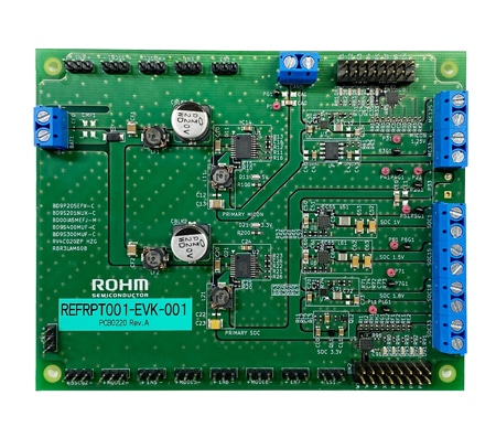
The power tree board for automotive infotainment/ADAS integrates functional safety features, ensuring EMC compliance with supervisor ICs for reliability and space-saving.
CISPR 25 Class 5 compliance is crucial in automotive electronics due to the growing complexity of vehicle systems and the need to ensure they do not interfere with each other or external devices. Compliance ensures Electromagnetic Compatibility (EMC), preventing excessive electromagnetic interference (EMI) that could disrupt other systems or pose safety risks. Meeting EMC standards improves system reliability and safety, as EMI can lead to malfunctions or failures in critical systems. Regulatory compliance is another key driver, as adherence to standards like CISPR 25 is often required for certifications and approvals. In the challenging automotive environment, with various sources of EMI, compliance helps systems operate reliably. Non-compliance can lead to legal issues, making adherence to standards essential for automotive manufacturers.
The reference design from ROHM Semiconductor is a power tree solution board tailored for infotainment devices like automotive clusters, center information displays, and ECUs for ADAS applications. It integrates a power system capable of supporting functional safety onto a single board, optimizing the configuration as a power tree. The design ensures excellent EMC performance, meeting CISPR25 Class 5 standards across all power supply rails, while also reducing heat generation through the distribution of high-efficiency DCDCs. Additionally, two supervisor ICs with self-diagnosis functions can monitor the output of all power rails, enhancing functional safety.
The Automotive Infotainment/ADAS 8-channels power tree reference design has been verified to meet the EMC CISPR 25 class 5 standard, even without a common mode filter. To prevent interference with AM radio frequency bands, all DC/DC converters operate at a switching frequency of 2.2 MHz or higher. The thermal characteristics have been thoroughly tested, and voltage monitoring for the 8-channel power tree has been implemented to enhance functional safety to ASIL level standards. Additionally, space-saving features have been incorporated by integrating multiple power trees into the design.
The REFRPT001-EVK-001 features two power supply monitoring ICs, each dedicated to monitoring the DCDC_P5V and DCDC_P3V system power trees. These ICs provide Power Good signals, XRSTOUT signals, and Watchdog Timer outputs, which can be monitored using Monitor-terminal-1 / -2. The output signals of the power monitoring ICs can be verified using LED.
ROHM Semiconductorhas tested this reference design. It comes with a Bill of Material (BOM), schematics, Printed Circuit Board (PCB) layout, etc. You can find additional data about the reference design on the company’s website. To read more about this reference design, click here.
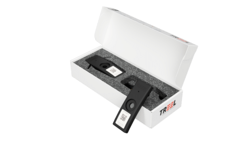
The tire pressure monitoring system boosts road safety and vehicle efficiency and extends battery life with innovative sensor technology.
TREEL Mobility Solutions, a provider of automotive technologies, focuses on enhancing road safety and boosting efficiency in vehicles, tires, and fuel through its ‘Tire Pressure Monitoring Solution’ (TPMS). This system handles different pressure levels, excessive vibration, and temperature fluctuations. It’s suitable for a wide range of vehicles, including two- and four-wheel vehicles, buses, and both light and heavy commercial vehicles, as well as for off-road use. After over four years of production, the system has evolved to align with the market for tire monitoring.
The TPMS is offered in three models. The first variant consists of sensors fitted to each tire, including the spare, to monitor pressure and temperature. Each sensor utilizes the Nordic Semiconductor nRF52810 SoC, powered by an Arm® Cortex-M4 processor, to oversee the system.
The second variant integrates these sensors with a Bluetooth device acting as a central and peripheral unit. It features a multiprotocol radio that sends data to an nRF52832 SoC via Bluetooth® LE. This SoC then relays the tire pressure and temperature data directly to the vehicle’s Controller Area Network (CAN) or a mobile app for user notification.
The third variant includes the sensors and a ‘TREEL Mobility Solutions TPMS Receiver’. This receiver uses the nRF52833 SoC to gather data and displays tire status through a separate screen unit.
The ‘Smart Tire’ app, available for iOS and Android, allows users to set alarms that notify them of deviations in tire pressure from set levels. The app lets users adjust transmission frequencies and configure active and sleep modes to enhance battery efficiency. The extended battery life is due in part to the low power consumption of the Nordic SoC. The nRF52810 SoC is designed to minimize power usage, featuring a 2.4 GHz radio with low peak RX/TX currents and an automatic power management system.
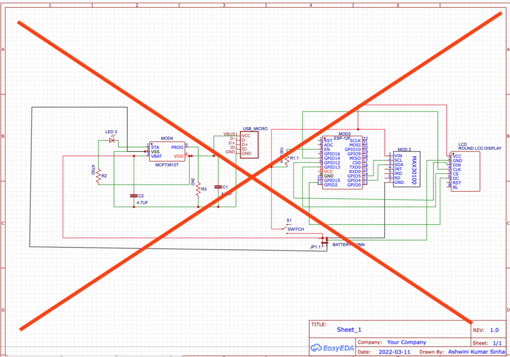
Nets are transforming electronics design! From messy wire connections to organised circuits, learn why professionals are making the switch.
Schematic circuit design is a key step for any electronics product design, which we later convert to PCBs and then generate the Gerber files for PCB production. However, the circuit diagrams and designs we often see during our engineering days look something like Fig. 1, with wires to show connections. Yet, when you transition to the professional world and delve into complex designs, you encounter designs like the one in Fig. 2.
Most professional circuit designs and reference designs often resemble this. Many engineers, especially those who are self-taught or lack formal training in electronics design, may not be aware of this design, which uses nets.
For basic circuit design, the first option is acceptable. However, for professional product design and prototyping, if you need to make changes to the design and replace any ICs, or diodes, it becomes a complex problem.
Making such changes in the initial design, where we have wire lines to connect the pins and components on the circuit, can be challenging. If your design has many components, a mesh of wire lines makes it complex to read the design.
It also becomes impossible to change or replace the ICs and components in the design. Many newbies and amateur design engineers unknowingly make this mistake and find themselves in a difficult situation when their design requires modification or updating.
This article is for those design engineers, especially those new to electronics design, who may have entered electronics design as hobbyists and learned through experience rather than pursuing a certification course in circuit design.
Recently, I published a RISC-V system design using the nets-based design and received numerous messages from people who were unaware of it and unable to read the circuit design I published.
WHERE IS THE REST OF THIS ARTICLE'S CONTENT?
This is PREMIUM content, which means that only
REGISTERED users of our website can read it, by logging in.
If you ARE a registered user, CLICK HERE to login.
Else, CLICK HERE to register for FREE!
Are you tired of losing your keys, bags, or other valuable belongings? Say goodbye to those worries with our step-by-step guide to creating your very own Enhanced AirTag! This innovative device utilizes WiFi technology to provide extended-range coverage and detailed tracking data, all at an affordable price point.
Materials Required:
IndusBoard Coin: 1 unit – This compact board features built-in Wi-Fi and necessary sensors, making it perfect for our AirTag project.
3.3V Rechargeable Battery: 1 unit – Provides the necessary power for the device.
USB to UFL Antenna Cable: 1 unit – Enhances WiFi range and accuracy.
Fig 1. Air tag showing distance and direction on the phone
Step-by-step Guide to Building AirTag using IndusBoard
Step 1: Setting Up the Hardware
Connect the 3.3V rechargeable battery to the IndusBoard Coin. Ensure the positive (red) and negative (black) terminals are properly aligned.
Attach the USB to UFL antenna cable to the UFL antenna connector on the IndusBoard Coin. This will enhance the WiFi range and accuracy of your AirTag.
Step 2: Configuring the Software
Open the Arduino IDE on your computer and load the provided code for the Enhanced AirTag project.
Configure the SSID and password for your phone’s hotspot in the code. This will allow you to access the device’s user interface (UI) for tracking purposes.
Implement data monitoring from the magnetometer accelerometer to capture movement, motion tracking, and direction information.
Create a web server page in the code to update real-time tracking data. Additionally, include a function to check WiFi connectivity with the device for seamless connection.
Fig 2. Getting direction from magnetometer 3D axis value
Step 3: Uploading the Code
Connect the IndusBoard Coin to your computer using a USB cable.
Upload the configured code to the device using the Arduino IDE.
Monitor the serial output in the Arduino IDE to ensure the code is uploaded successfully and check the connection status.
Fig 3. Code snippet for the webpage
Step 4: Testing the Device
Disconnect the USB cable and connect the 3.3V rechargeable battery to the IndusBoard Coin.
Monitor the serial output for the device to connect to your phone’s WiFi hotspot. Note down the IP address displayed in the serial monitor.
Access the device’s web server through your phone’s browser using the IP address noted earlier.
Explore the web interface to view real-time tracking data, including direction, distance, and movement.
Step 5: Fine-tuning and Optimization
Experiment with different antenna configurations to optimize WiFi range and accuracy.
Implement additional features or functionalities in the code to enhance the device’s capabilities.
Test the device in various scenarios and environments to ensure its reliability and effectiveness.
Fig 4. IndusBoard-based AirTag Serial MonitorFig 5. AirTag Data Monitoring
Congratulations! You’ve successfully built your own Enhanced AirTag with extended range capabilities. With its comprehensive tracking data and affordable price, this DIY project is sure to revolutionize the way you track your belongings. Enjoy peace of mind knowing that your keys, bags, and other valuables are always available.
Below You can check the Complete Video Tutorial to make this Low-cost AirTag from the Scratch.


 A Mini Fridge that can work with any power bank and without using harmful CFC gases.
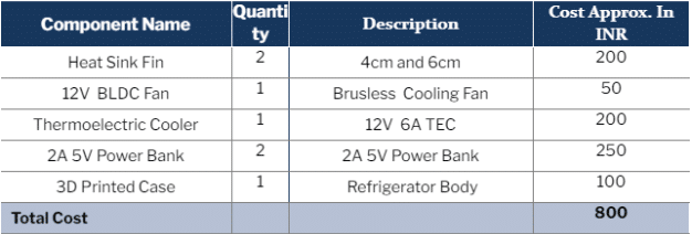


 -M4 processor, to oversee the system.