What is Atmega Atmel AVR Microcontrollers ?
Introduction to ATMega Microcontrollers
ATMega Microcontrollers belong to the AVR family of microcontrollers and is manufactured by Atmel Corporation. An ATMega Microcontroller is an 8-bit microcontroller with Reduced Instruction Set (RISC) based Harvard Architecture.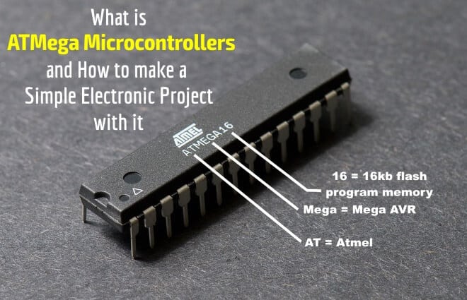
As the name suggest, for instance, “ATmega16″ , where AT = Atmel, mega = mega AVR and 16= 16kb flash memory.
It has standard features like on-chip ROM (Read Only Memory), Data RAM (Random Access Memory), data EEPROM (Electrical Erasable Programmable Read Only Memory), Timers and Input / Output Ports, along with extra peripherals like Analog to Digital Converters (ADC), Serial Interface Ports etc. They have 120 and more instruction set and program memory ranges from 4K to 256K Bytes.
History of ATMega Microcontrollers
The ATMega microcontrollers were designed by two Norwegian Institute of Technology (NTH) students – Alf-Eigel Bogen and Vegard Wollan. It was later bought and developed by Atmel Corporation in 1996.
Architecture of ATMega Microcontrollers
As mentioned in the introduction part, ATMega microcontrollers are based on Harvard architecture, i.e. separate data memory and program memory. The Program memory also known as Program or Code Memory is the Flash Random Access Memory (ROM). The size of program memory ranges from 8K to 128K Bytes.
The data memory is divided to three parts – 32 General Purpose Registers, Input/output memory and Internal Static Random Access Memory (SRAM). while the size of General Purpose Registers is fixed, the I/O Memory and internal SRAM size varies from chip to chip.
Block Diagram of ATMEGA Microcontroller
The below diagram represents the architecture of ATMega microcontrollers.
Click image to enlarge

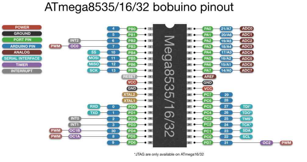
Pinouts & Modules of ATMega microcontroller
Click image to enlarge
 Let us have a brief overview about each and every module
1. General Purpose Registers: The ATMega microcontrollers have register based architecture, i.e. both the operands and the result of operations is stored in the registers, collocated with the Central Processing Unit (CPU). The general purpose registers are coupled to the processor’s Arithmetic Logic Unit (ALU).
These registers are used to store information temporarily while executing a program. These consume 32 Bytes of Data Memory space and takes the address location – $00 to $FF. These registers are nomenclature as R0 to R31 and are each 8-bit wide.
2. Input / Output Memory: This is also referred to as Special Function Register (SFR) memory as it is dedicated to special functions like status registers, timers, serial communications, I/O ports, Analog to Digital Counters (ADC), etc.
The number of locations occupied by this memory depends on the number of pins and peripheral functions supported by the chip. While 64 Bytes of I/O location is fixed for all chips, some ATMega microcontrollers have an extended I/O memory which contains registers related to the extra ports and peripherals.
3. Internal SRAM: This is also referred to as scratch pad and is used to store data and parameters by programmers and compilers. Each location is accessible directly by its address. This is used to store data from Input / Output and serial ports into the CPU.
4. Flash Electrically Erasable Programmable Memory (Flash EEPROM): This is an in-system programmable memory used to store the programs. It is erasable and programmable as a single unit. Since it is non-volatile, memory content is retained even in case of power off. For each ATMega microcontroller, the number at the end of the name denotes the capacity of flash memory.
For example, for ATMega16, the flash memory capacity is 16K Bytes. An advantage of flash memory in ATMega microcontrollers is its in-system programmability, i.e. the microcontroller can be programmed even while being on the circuit board.
5. Data Electrically Erasable Programmable Memory (Data EEPROM): Some This memory is used to store and recall permanent program data and other system parameters.
- Also Read: What is ZigBee Technology and How it works?
Apart from the memory module, the microcontroller external connections for power supplies, two external crystal input pins, processor reset and four 8-bit ports.
1. Ports: The ATMega microcontrollers contain four 8 bit ports – Port A, Port B, Port C and Port D. Each port is associated with three registers – Data Register (writes output data to port), Data Direction Register (sets a specific port pin as output or input) and Input Pin Address (reads input data from port).
2. Clock: Microcontroller clock is used to provide time base to the peripheral sub systems. We can set clock internally by using the user-selectable Resistor Capacitor or externally using oscillators.
3. Timers and Counters: ATMega microcontrollers generally contain 3 timers/counters. While two 8-bit timers can also be used as counters, the third one is a 16-bit counter. These are used to generate precision output signals, count external events or measure parameters of input digital signal.
3. Serial Communication Systems: ATMega microcontroller chip contains in-built Universal Synchronous and Asynchronous Serial Receiver and Transmitter (USART), Serial Peripheral Interface (SPI) and Two Wire Serial Interface (TWI).
4. Analog to Digital Converters: ATMega microcontrollers contain multi-channel Analog to Digital Converter (ADC) subsystem.The ADC has 10-bit resolution and works on the principle of successive approximation. It is associated with three registers –ADC Multiplexer Selection Register, ADC Control and Status Register, and ADC Data Register.
5. Interrupts: There are 21 interrupt peripherals in ATMega microcontrollers. While 3 are used for external sources, remaining 19 are used for internal sub-systems. These are used to interrupt normal sequence of events in case of high priority emergencies.
Programming in ATMega Microcontrollers
As mentioned earlier, ATMega microcontroller is based on RISC architecture, i.e. it contains reduced set of instructions. Similar to other microcontrollers, programming in ATMega microcontrollers can also be done in both low level languages (assembly) or high level languages (Embedded C).
Let us have a brief discussion about assembly level programming.
An assembly language instruction consists of the following fields:
[Label: ] mnemonic [operands] [; comments]
Here mnemonic refers to the instruction. ATMega microcontrollers support both immediate as well as indirect addressing modes. The I/O registers can be accessed through their respective locations in the memory space.
Operands refer to the arguments operated on by the instruction. For ATMega microcontrollers, the operands are the general purpose registers or the I/O registers.
Generally programming is done using C language owing to the simplicity. Given below is a small example of programming ATMega16 microcontroller using C language
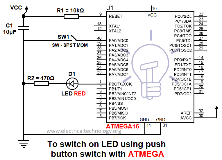
Circuit Diagram of Simple LED Project with ATmega16 Microcontroller
Purpose: To switch on LED using push button switch with ATmega16 Microcontroller
 Project Code:
{
DDRA=0x00;
DDRB=0xFF;
unsignedinti;
while(1)
{
i=PINA;
if(i==1)
{
PORTB=0xFF;
}
else
PORTB=0x00;
}
}
In the above code, I have assigned Port A as input port, of which Pin PA.0 is connected to a push-button switch. Port B is assigned output port, of which Pin PB.0 is connected to LED.
I have written and compiled the code using Atmel Studio 7, which converts the .c file to binary ELF object file. It is then again converted to hex file, which is passed to the microcontroller using AVRdude program.
This is a brief information about ATMega microcontrollers. Any other related information is welcome in the comments below.
You may also read:
- What is Raspberry Pi? Creating Projects using Raspberry Pi
- What is PID Controller & How it Works?
- Programmable Logic Controllers (PLC) for Industrial Control
The post What is ATMega Microcontrollers & How to Make an LED Project with it? appeared first on Electrical Technology.
January 23, 2018 at 07:11AM by Department of EEE, ADBU: http://ift.tt/2AyIRVT