Digital Binary Adder & Subtractor
What is Binary Adder ?
A digital binary adder is a digital device that adds two binary numbers and gives its sum in binary format.
The two numbers to be added are known as “Augand” and “Addend”. The first number in addition is occasionally referred as “Augand”.
Digital adders are mostly used in computer’s ALU (Arithmetic logic unit) to compute addition. Digital calculators use adders for athematic addition. Micro controllers use adders in arithmetic additions,PC (program counter) and timers etc. Every device that uses some kind of increment or arithmetic process contains adders.
The building block of digital adder is Half Adder. Half adders come together to form full adder.
We will briefly discuss them one by one.
- You may also read: Ripple Carry And Carry Look Ahead Adder
Types of Binary Adder & Subtractor
- Half Adder
- Full Adder
- 4 Bit Adder
- Subtractor
- Adder / Subtractor
We will discuss one by one as follow:
Half Adder
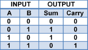
Half adder can add 2 single bit numbers.
Consider the two numbers A, B, and the output being “Sum” and “carry”.
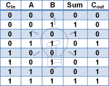
Truth Table
The truth table of half adder is given below.
Half Adder using Discrete Logic Gates
Sum
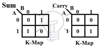
According to the truth table of half adder and the K-map, the SOP expression for “Sum” is:
Sum = A̅B + AB̅
Schematic for “Sum” using discrete logic gates is given below.
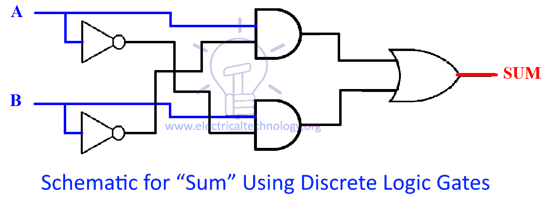
The expression for “Sum” is same as XOR with input A and B so it can be replaced with a single XOR gate as shown below:
Sum = A XOR B

Carry
According to the truth table of half adder the SOP expression for “Carry” is:
Carry = AB
“Carry” is AND of input A,B as shown below.

Construction of Half Adder
Complete half adder is made by combining “sum” and “carry” schematic as shown in figure below;

Half Adder using Universal Gates
Half Adder using NAND Gates
NAND gate is a Universal gate which means any kind of logic gate or function can be implemented with NAND gate.
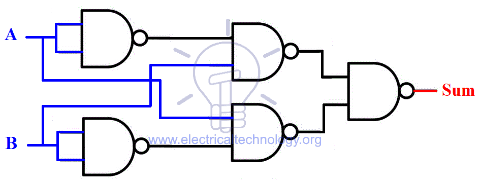
SOP (Sum of products) expression can easily get implemented with NAND gates.
Sum
SOP expression for“Sum of half adder”.
Sum = A̅B + AB̅
(Sum)’ = (A̅B + AB̅)’
(Sum)’ = {(A̅B)’ & (AB̅)’}
(Sum)’ = [ { (A &A)’&B}’ & {A &(B & B)’}’]
Sum = [ { (A &A)’&B}’ & {A &(B & B)’}’]’
- You may also read: Digital Flip-Flops – SR, D, JK and T Flip Flops
This expression for “sum” can be implemented using NAND gates as shown below:
Carry
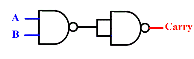
SOP expression for “half adder’s carry” output is :
Carry = AB
(Carry)’ = (AB)’
Carry = (AB)’’
In other word INVERT of NAND gate is AND gate, and schematic of “Carry” using NAND gate is given below.
Half adder
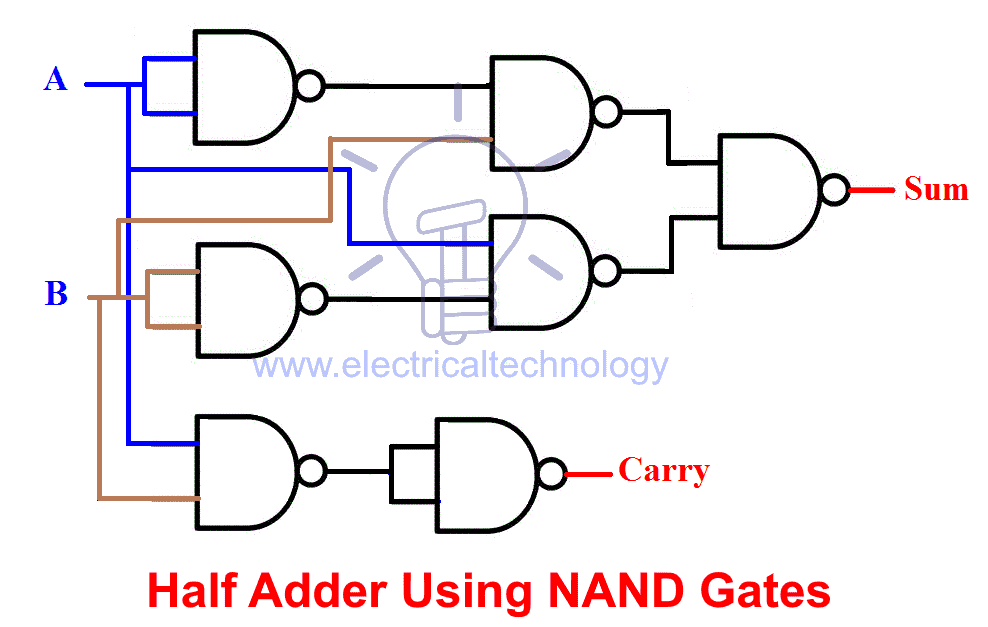
NOW we will combine these two schematics to make half adder using NAND gates.
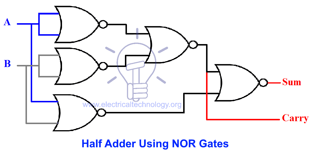
Half Adder using NOR Gate
NOR gate is also a universal gate and POS (product of sums) expressions can easily be implemented using NOR gates.
Sum
According to half adder truth table, POS expression for the sum is:
Sum = (A̅+B̅) & (A+B)
(Sum)’ = {(A̅+B̅) & (A+B)}’
(Sum)’ = {(A̅+B̅)’ + (A+B)’}
Sum = {(A̅+B̅)’ + (A+B)’}’
Sum = [{(A+A)’+ (B+B)’}’ + (A+B)’]’
Schematic of “Sum” using NOR gates are given below:

- Also read: Comparator and Digital Magnitude Comparator
Carry
Expression for “carry” is
Carry = AB
(Carry)’ = (AB)’
(Carry)’ = (A’+B’)
Carry = (A’+B’)’
Carry = {(A+A)’+(B+B)’}’
The schematic for “Carry” using NOR gates is given below:

Half adder Schematic using NOR Gates
Now if we combined these two schematics together it will form half adder using NOR gates.
Half adder can add only two 1-bit numbers and it cannot add the third number (carry) which comes from previous numbers addition which is why it is known as HALF ADDER.
It cannot be used for addition of more than 1-bit.
Full Adder
A full adder can add numbers with carry from previous additions.
It consists of 3 inputs. 2 inputs being “Augend” and “addend” and the third one is “carry in” from previous additions.
It has 2 output;“Sum” and Cout as carry out.
Consider 2 numbers A,B, and Cin as input and “sum”, Cout as output.
Truth Table
Truth table of full adder is given below;
Sum
According to the truth table of a full adder, the SOP expression for “Sum” is:
Sum = C̅inA̅B + C̅inAB̅ + CinA̅B̅ + CinAB
Sum = C̅in(A̅B + AB̅) + Cin(A̅B̅ + AB)
Sum = C̅in(A XOR B) + Cin(A XNOR B)
Sum = C̅in(A XOR B) + Cin(A̅̅ X̅O̅R̅̅ B̅)
Sum = CinXOR (A XOR B)
Schematic Diagrams of Full Adders
According to this expression schematic for full adder’s Sum is.

According to Karnaugh’s map for Sum given below, there is no pair so the expression will be same and cannot be minimized;

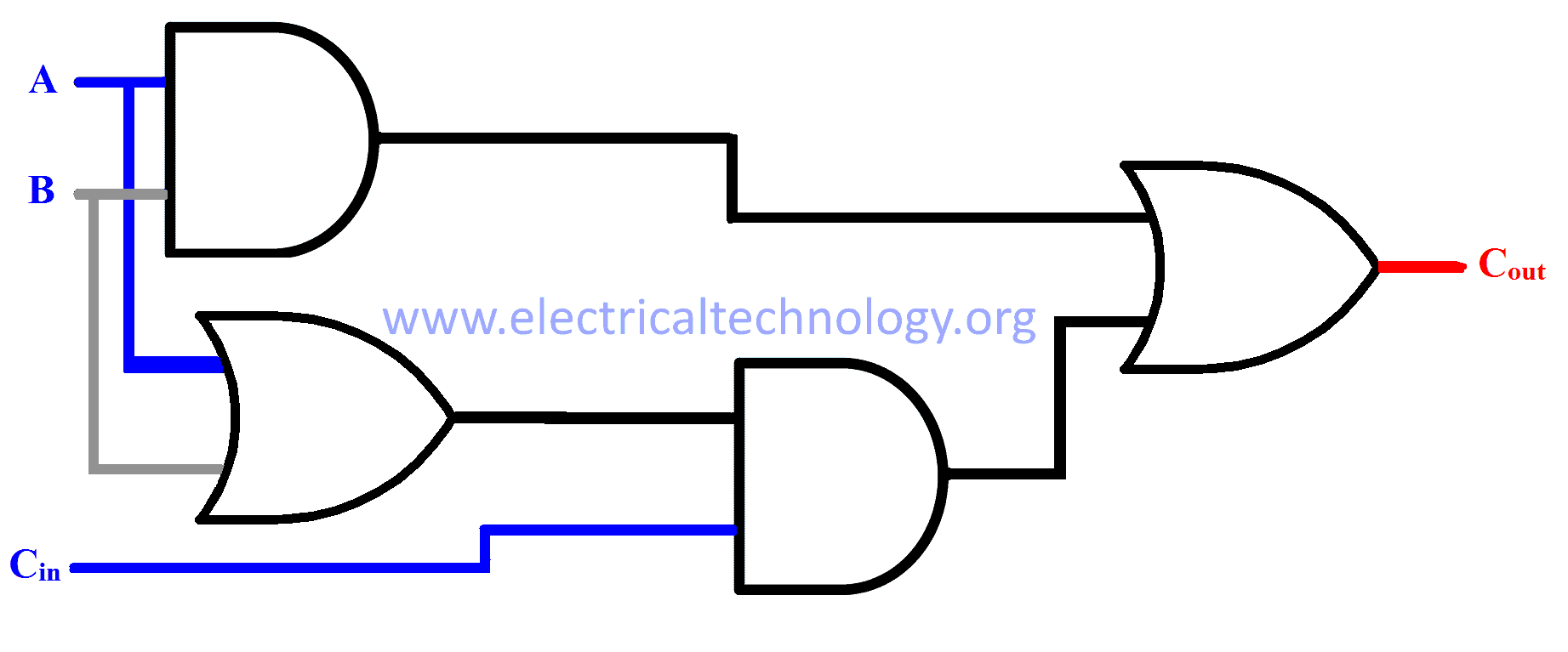
Carry out
Full Adder using truth table
According to the full adders truth table, SOP expression for Cout is
Cout = C̅inAB + CinA̅B + CinAB̅ + CinAB
Cout = C̅inAB + CinAB + CinA̅B + CinAB̅
Cout = AB(C̅in + Cin) + Cin(A̅B + AB̅)
Cout = AB + Cin(A XOR B)
Schematic for Cout is given below

Full Adder using Karnaugh Map
According to karnaugh’s map for Cout the expression will be:

Cout = AB + CinB + CinA
Cout = AB + Cin(A+B)
Schematic for Cout using karnaugh map’s expression
The schematics of Full adder are shown in the figures below:
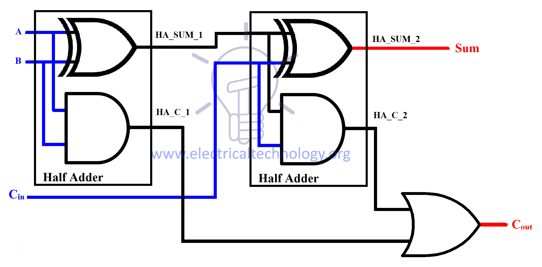
Full Adder using individual half adders
A full adder can be implemented using two half adders in cascaded setup.
A half adders output is:
HA_Sum = (A XOR B) = A̅B + AB̅
HA_C = AB
Half adder sum is denoted by HA_sum and carry out is denoted by HA_C
Full adder output expression is:
Sum = CinXOR (A XOR B)
Sum = CinXOR (HA_sum_1) (HA_sum_1; sum of first half adder whose input is A,B)
Sum = HA_sum_2 (HA_sum_2; sum of second half adder whose input is HA_sum_1 and Cin)
Cout = AB + Cin(A XOR B)
Cout = AB + Cin(HA_sum_1)
Cout = HA_C_1 + HA_C_2 (HA_C_1; carry out of first adder whose input is A,B
HA_C_2; carry out of the second adder whose input is Cin,HA_sum_1)
According to the equation of Sum and Cout. the schematic of a full adder using half adder is given below.
Full Adder using universal gates
Full Adder using NAND Gates
We have designed half adders using NAND gates.
We will use NAND gate half adder in the cascaded setup as discussed above.
Sum = Sum of second half adder
Cout = HA_C_1 + HA_C_2
Cout’ = (HA_C_1 + HA_C_2)’
Cout’ = (HA_C_1)’ & (HA_C_2)’
Cout = {(HA_C_1)’ & (HA_C_2)’}’
In “NAND half adder carry out” schematic, “carry out” has been inverted at the end. We will bypass the inverter and feed it to NAND gate as shown in the expression above.

Full adder using NOR Gates
For NOR gate we will use NOR gate half adders.
Sum = Sum of second half adder
Cout = HA_C_1 + HA_C_2
Cout’ = (HA_C_1 + HA_C_2)’
Cout‘’ = (HA_C_1 + HA_C_2)’’
Thus the schematic for Full adder using NOR gate will be :
 These full adders can be used for adding ‘n’ bit number sif ‘n’ number of full adders are connected in a cascaded setup with cout connected to the Cin of the next full adder.
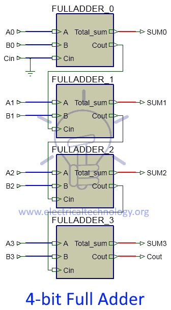
4-bit Full adder
‘n’ bit adder can be made using ‘n’ full adders in series. This way, 4-bit adder can be made using 4 full adders.
Each full adder for separate bit addition and Cout of one adder will be fed to the succeeding adder’s Cin and the last Adder’s Cout will be the Cout of 4-bit adder.Each full adder will give single bit of Sum as output.
The Cin of the first Full adder will be hard wired to the ground (0).
Digital Binary Subtractor
A combinational digital device capable of subtracting the second binary number forms the first one is called digital Subtractor.
First, we will discuss how subtraction works.
Consider two numbers A and B being subtracted.
OUT = A – B
OUT = A + (-B)
This equation means that these numbers are added together like in adder but the second number is negative of itself.
In Binary system the negative of a number is 2’s complement of that number.
To take 2’s complement of a number; first, we need to invert all the bits of that number this inversion is known as 1’s complement. And then add 1 with it as shown below.
B = B3B2B1B0
1’s complement B = B̅3B̅2B̅1B̅0
2’s complement B = B̅3B̅2B̅1B̅0 + 1
The MSB of signed number is sign bit. It is 1 for negative sign and 0 for positive,
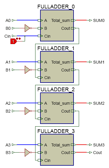
Thus we need to invert the 2nd input of Adder and set Cinto “1” to get added in B for subtraction as shown in the figure below.
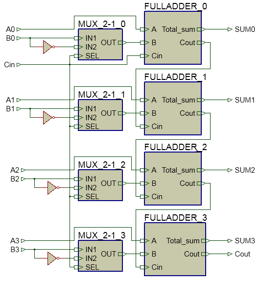
We can use adder as subtractor if we make Cin input as a selector between addition and subtraction. And we use a multiplexer (input line selector) for the second input.
If Cin is low ”0” ; it will select B as input thus addition will occur.
If Cin is high ”1” ; it will select B̅ as input and Cin will get added in, thus subtraction will occur.
Schematic of Half and full Subtractor
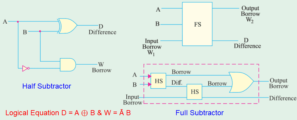
Logical Equation for Half Adder and Full Adder.
D = A ⊕ B and W = Ā B
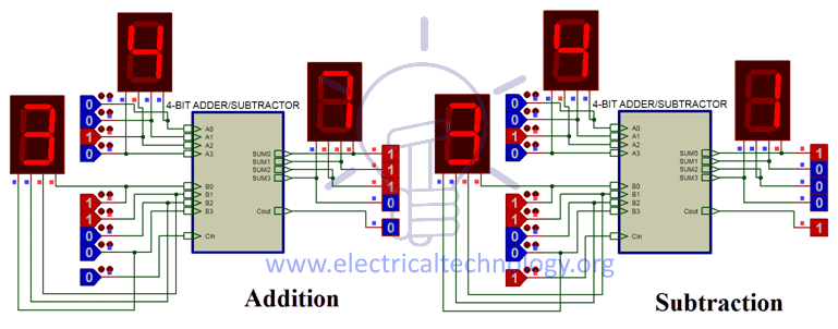
Adder and Subtractor
Simulation diagrams of Adder and Subtractor is given below.
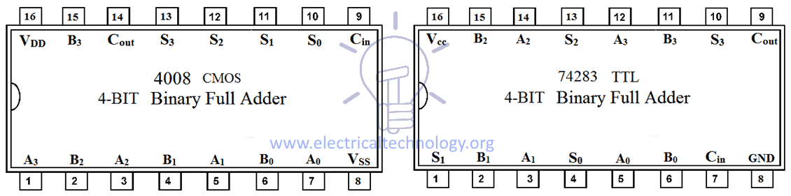
Binary Adder IC Configuration & Pin out.
Some of Adder ICs with pin configuration is given below:
- 4008 CMOS 4-BIT Binary Full Adder
- 74283 TTL 4-BIT Binary Full Adder
Applications of Adders and Subtractor
- Adders & Subtractors are wildly used in in computer’s ALU (Arithmetic logic unit) to compute addition as well as CPU (Central Processing unit) and GPU (Graphics Processing unit) for graphics applications to reduce the circuit complexity.
- Adder and subtractor are basically used for performing arithmetical functions like addition, subtraction, multiplication and division in electronic calculators and digital instruments.
- Adders are used in digital calculators for arithmetic addition and devises that uses some kind of increment or arithmetic process
- They are also used in microcontrollers for arithmetic additions, PC (program counter) and timers.
- It is also used in processors to calculate address, tables and slimier operations
- It is also used in networking and DSP (Digital signal processor) oriented system
You may also read:
- Digital Logic OR Gate
- Exclusive-NOR (XNOR) Digital Logic Gate
- Logic NOT Gate – Digital Inverter Logic Gate
The post Binary Adder & Subtractor – Construction, Types & Applications appeared first on Electrical Technology.
May 22, 2018 at 01:42AM by Department of EEE, ADBU: https://ift.tt/2AyIRVT