Universal Digital Logic NOR Gate
What is Logic Nor Gate
NOR Gate is a digital logic gate (Also known as Universal gate) which gives output “1” only and only when all of its inputs are logic LOW state “0”.
NOR gate is invert of OR Gate. In other words, if we connect NOT gate to the output of OR gate that will become NOR gate.
NOR gate usually has 2 input And 1 output. But it can have as many inputs as you want according to the requirement. But it will only have 1 output. It is the reversal of OR Gate.
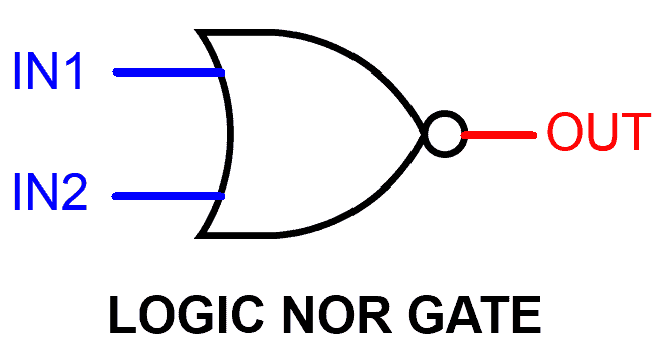
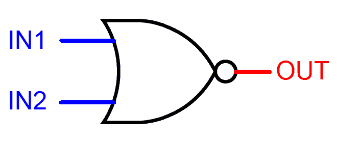
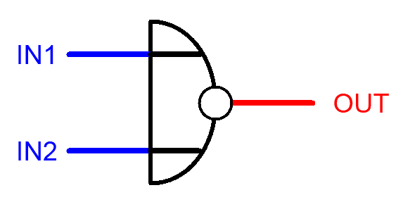
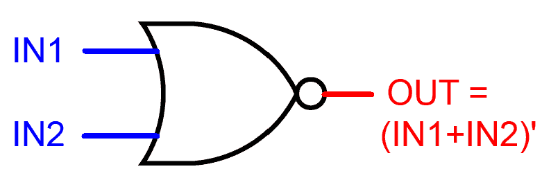
NOR Gate Logic Symbol, Boolean Expression & Truth Table
NOR Gate Boolean Expression
OUT = ( IN1 + IN2 )’
or ![]()
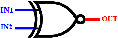
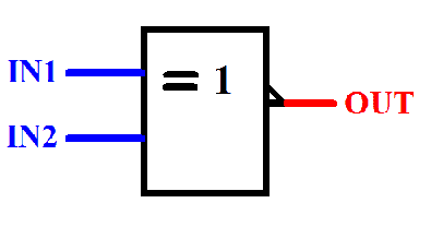
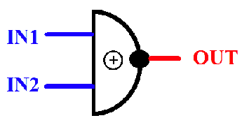
Symbol
There are 3 types of symbols used for NOR gate all over the world.
American National Standards Institute (ANSI)/ MILITARY
International Electrotechnical Commission (IEC)/EUROPEAN

Deutsches Institut für Normung (DIN)/GERMANY
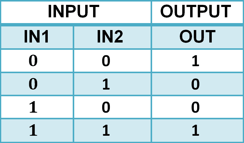
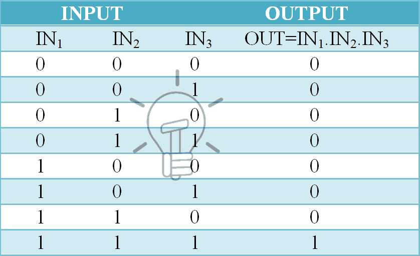
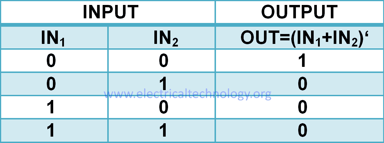
NOR Gate Truth Table
A mathematical table used to specify input to output logic combination of a digital circuit is known as a truth table, the truth table of NOR Gate is given below.
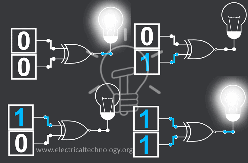
NOR Gate Logic Flow Schematic Diagram

NOR Gate Construction and Working Mechanism
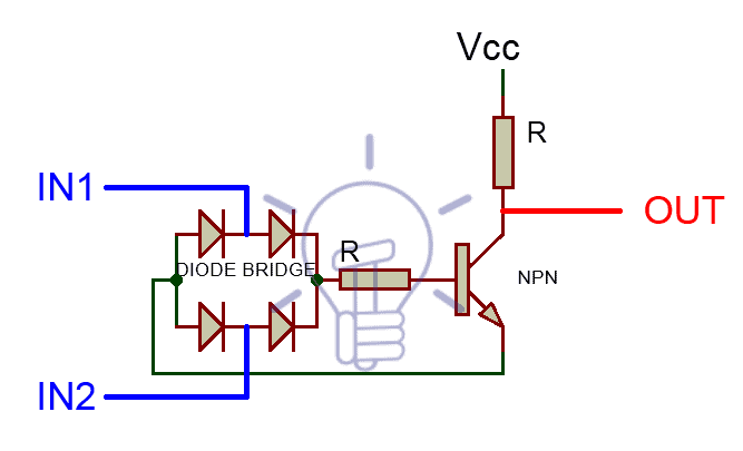
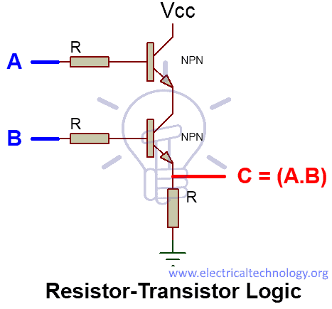
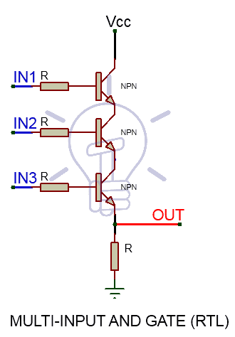
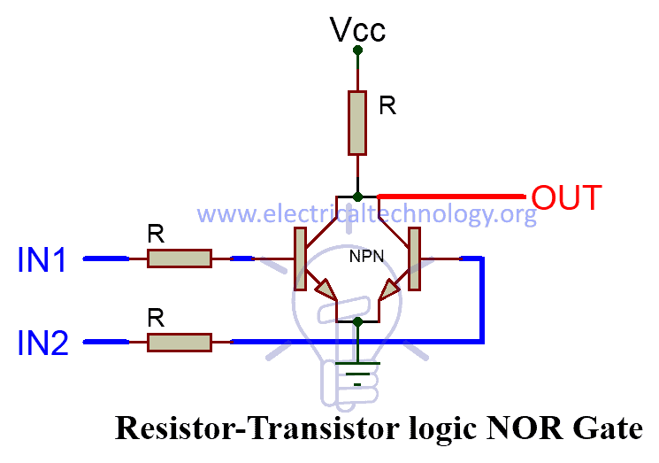
Resistor-Transistor Logic
In Resistor-Transistor logic (RTL), Bipolar junction transistor (BJT) are used as switching unit. In this schematic given below, we have used two NPN transistor connected together in parallel.
NPN transistor switch on when there is HIGH input “1“ at its base and they start conducting current. And when its base input is LOW state “0“ then it switches off.
When both of the inputs are LOW state “0“, the NPN connected in parallel will be switched off and the path to the GND will be cutoff. The only path for the current flow remain will be from Vcc to output. Which will flow out as HIGH state “1“.
If there is a single of both HIGH input, then the NPN transistor will turn on and the path to the GND will connect. GND (logic LOW state“0“) will flow out through output as “LOW state 0“. Thus resulting in a truth table given below.
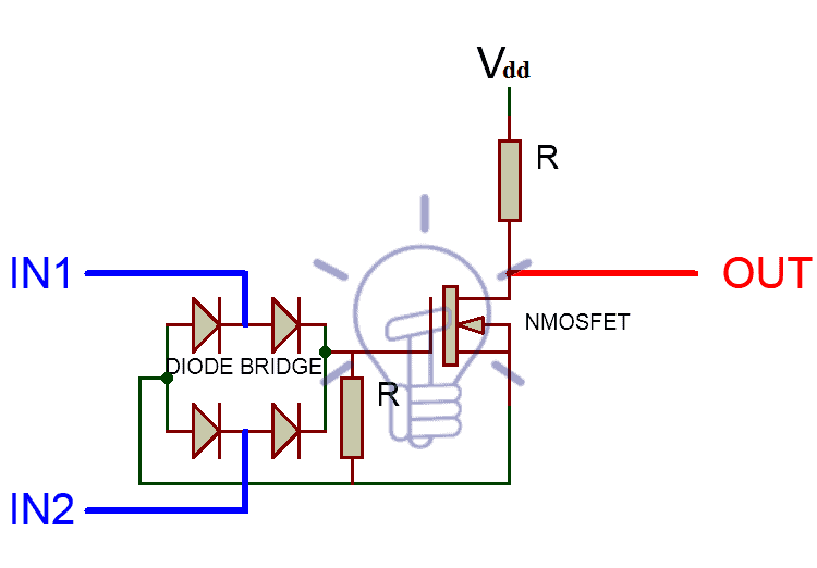
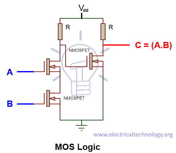
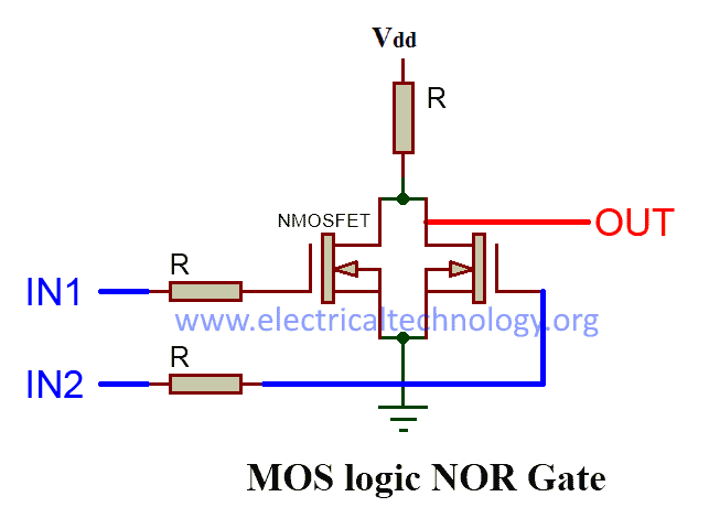
NOR Gate Mos Logic
MOS logic uses the idea of switching with MOSFETs instead of BJTs because of their High switching speed and low power consumption.
The schematic given in the figure below is a NOR gate using MOS logic, There are two NMOSFETs connected in aparallel configuration.
Its configuration and operation are exactly same as RTL logic NOR gate.
NMOSFETs also switch on when there is a HIGH state input at its gate(NMOSFET’s gate). And it switches off when there is LOW state input at its GATE.
When both of the inputs are LOW state “0“ the NMOSFETs will switch off and theonly path for current will be output thus resulting in HIGH state “1“ output.
And when one or both of the inputs are high state “1“ then NMOSFETs will switch on and GND to output path will connect, resulting in LOW state “0“ output.
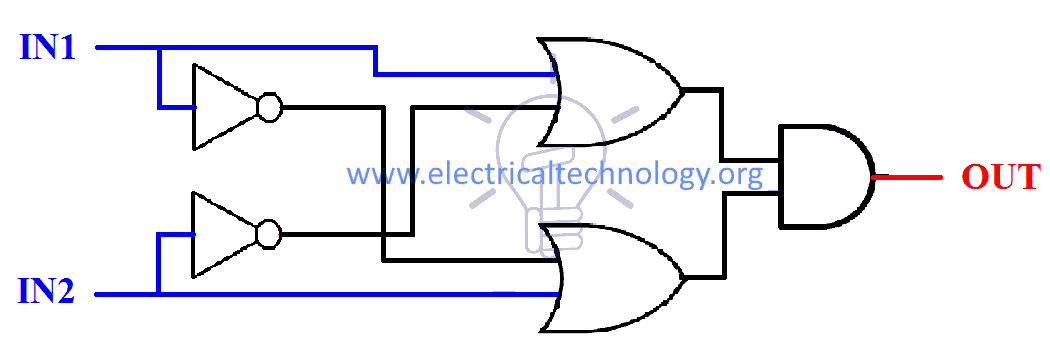
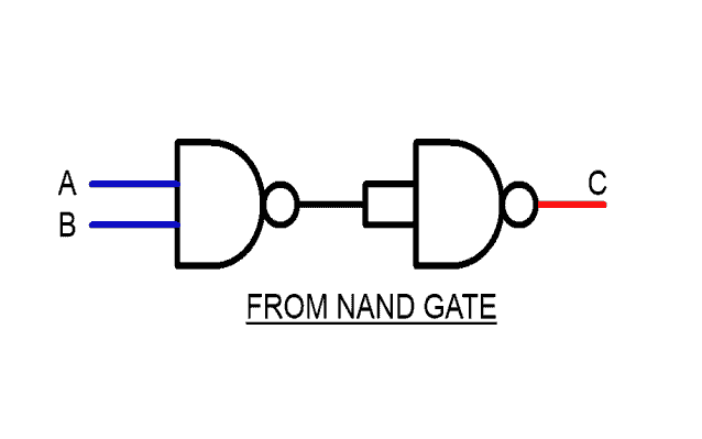
NOR Gate From Other Logic Gates
Universal gate NAND can be used as NOR gate if placed in a specific configuration shown in the figure given below. NOR gate can be made from OR,NOT gate as shown in the figure given below.
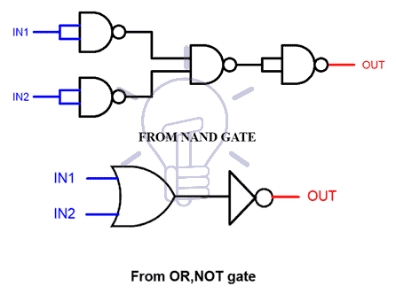
NOR Gate is a Universal Gate. A Universal gate is a gate which can be implemented into any other logic gate or logic function. Some of the basic gate’s implementation are given below.
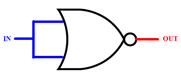
NOR Gate From NOT Gate
NOR gate can be used as NOT gate if we combine its input together into a single input.
In NOR gate all high state inputs lead to LOW output, and all LOW state inputs lead to HIGH input. Which is exactly the same as aNOTgate. NOT gate implementation diagram is given below.
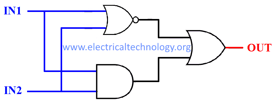
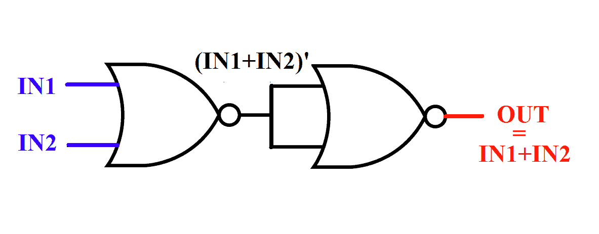
NOR Gate From OR Gate
NOR gate is opposite/invert of OR gate and viceversa. So inverting output of NOR gate will result in OR gate. To invert NOR gate output, we have to use NOR gate with combined inputs which work as Inverter/NOT gate.The figure of OR gate from NOR gates is given below.
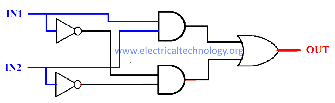
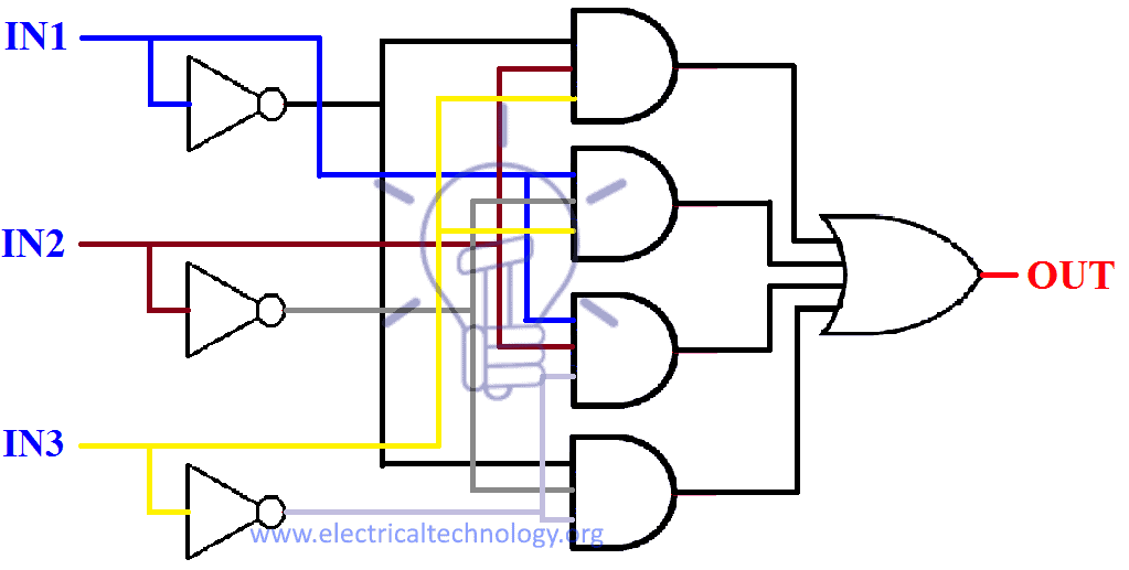
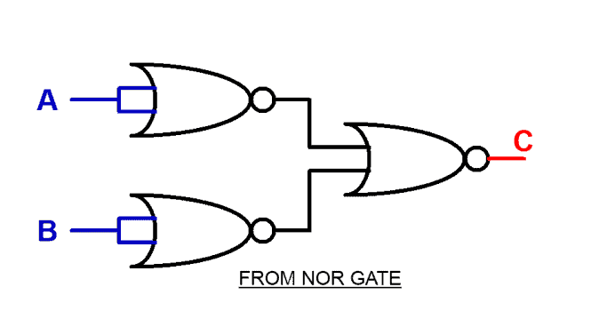
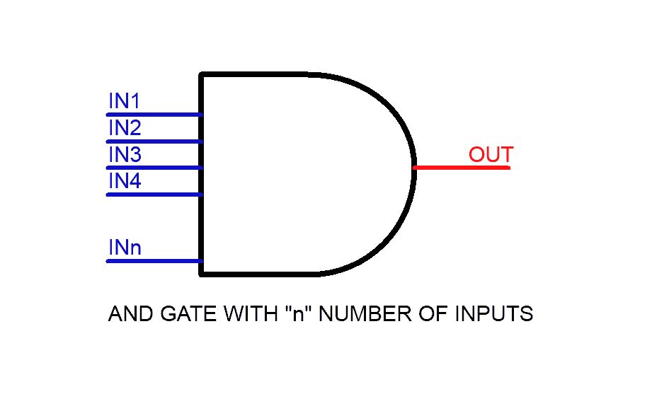
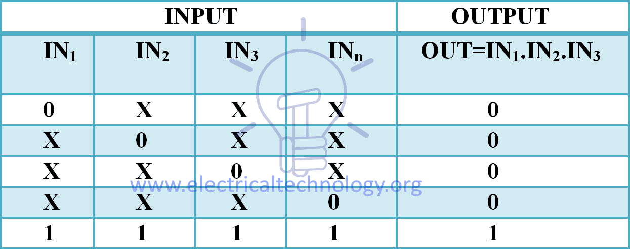
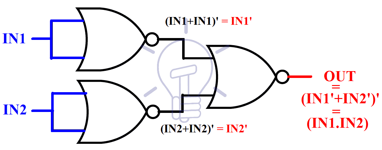
 NOR Gate From AND Gate
To better understand the implementation of AND gate using NOR gate one need to know about boolean algebra and De Morgans law.
Conversion of NOR to AND gate Boolean Algebraic expression is given below.
OUT = (IN1.IN2)
OUT‘ = (IN1.IN2)‘ taking complement on both sides.
OUT‘ = (IN1‘+IN2‘) De Morgans law
OUT‘‘ = (IN1‘+IN2‘)‘ taking complement on both sides.
OUT = {(IN1+IN1)‘+(IN2‘+IN2‘)}‘ as IN1= (IN1 + IN1)
So the end result is in the form of NOR gate. As you can see IN1,IN2 is NO Red with themselves and then they are NO Red with each other, to better understand look at the figure given below.
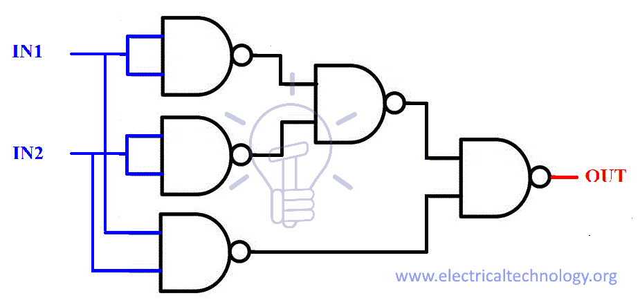
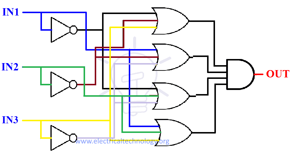
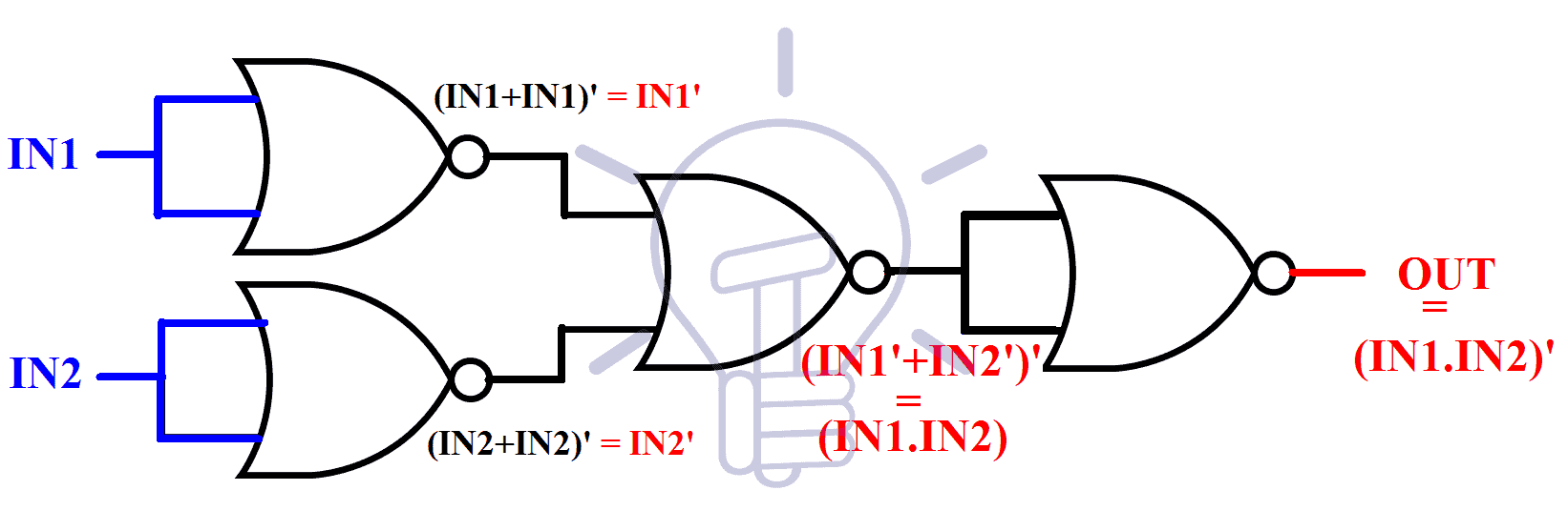
NOR Gate from NAND Gate
NAND gate is invert of AND gate. AND gate design will be the same as illustrated above. There will be an Inverter/NOT gate at the output of AND gate as shown in the figure given below.
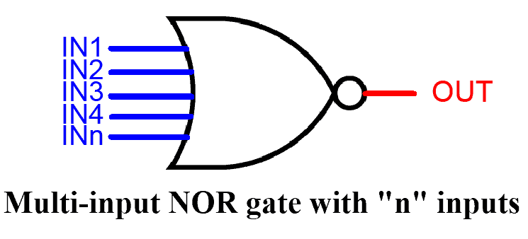
Multi-Input NOR Gate
NOR gate can have more than 2 inputs and can be used according to the requirements of the schematic design. The truth table of NOR gate with “n” number of input is given below.
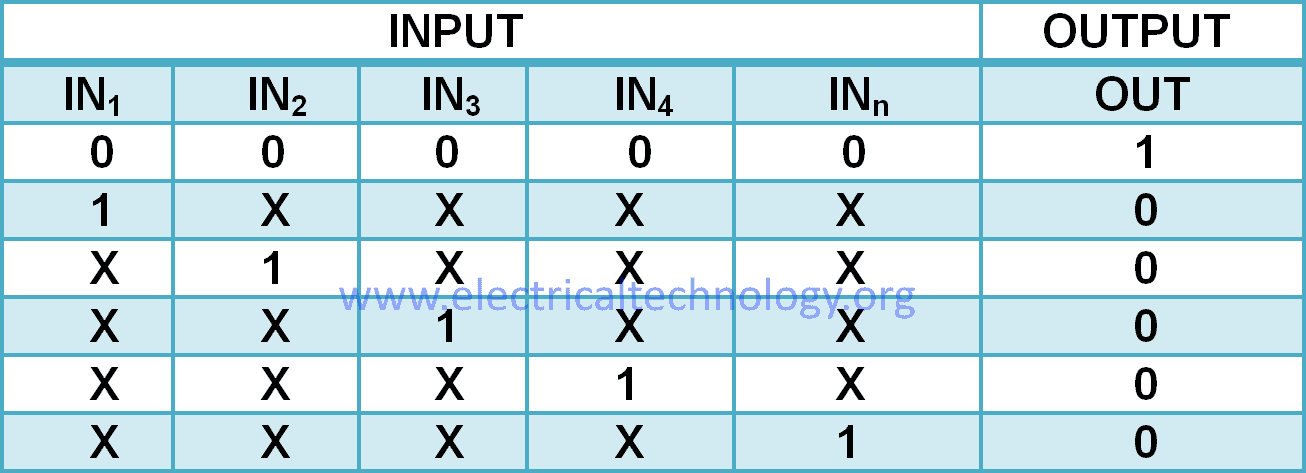
Truth Table
NOTE: In the table given above “X” means “don’t care”. It can be “1”and it can be “0”. Which means, as long as there is a single input carrying “1”, the output will be always “0” so there is no reason to put a check on other inputs, that’s why it’s called “don’t care X”.
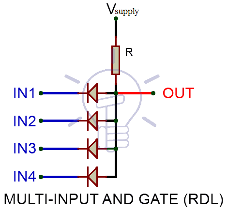
Resistor-Transistor Logic
In RTL (Resistor-Transistor Logic), Transistors are used as switching unit. To increase the input lines we have to increase the number of transistors connected in parallel as shown in the figure below.
![]()
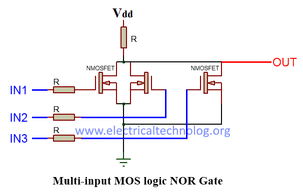
MOS Logic
The idea to create a Multi-Input NOR gate in MOS logic is exactly same as in RTL logic. Increasing the number of MOSFETs in parallel can potentially increase the number of input lines. The figure given below shows MOS logic NOR gate schematic.
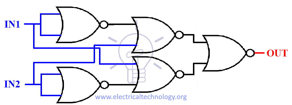
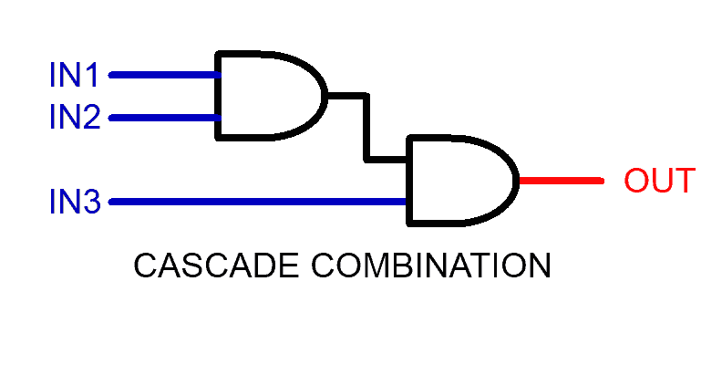
Multi-Input NOR Gate By Cascading 2-Input Gates
Multi-input NOR gate can be made from cascading setup of 2-input NOR gates as shown in the figure given below.
OUT = (IN1+ IN2 + IN3)‘
OUT = ((IN1 +IN2)’’ + IN3)’
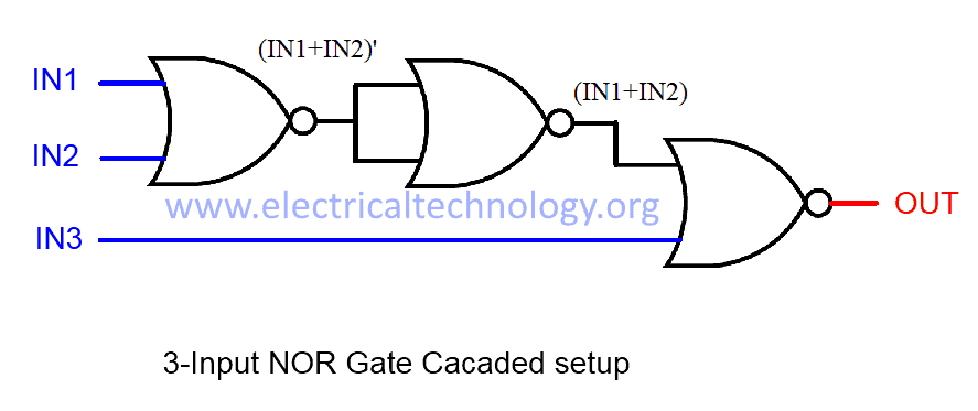 Since (IN1+IN2)‘‘ = (IN1+IN2)
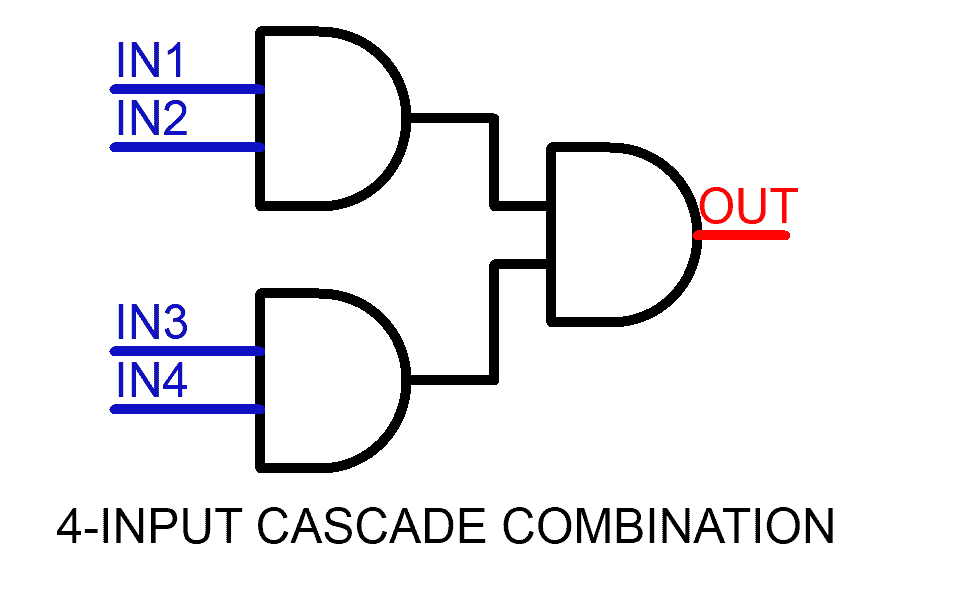
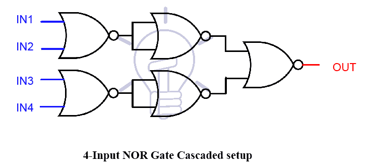
OUT = (IN1 + IN2+ IN3 + IN4)’
OUT = ((IN1 + IN2)’’ + (IN3 + IN4)’’)’
TTL and CMOS Logic NOR Gate IC’s
Commercially up to 8-input NAND gate’s IC are available in the market. Some of the commonly used IC’s details are given below.
TTL Logic NOR Gates
- 74LS02 Quad 2-input
- 74LS27 Triple 3-input
- 74LS260 Dual 4-input
CMOS Logic NOR Gates
- CD4001 Quad 2-input
- CD4025 Triple 3-input
- CD4002 Dual 4-input
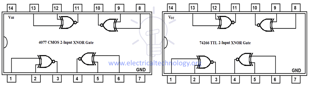
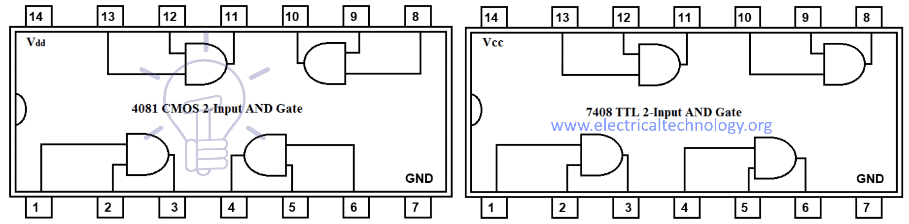
4001 CMOS and 7402 TTL 2-Input NOR Gate
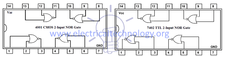
Pinout for 7402 TTL NOR Gate IC
| PIN Number | Description |
| 1 | Output Gate 1 |
| 2 | Input Gate 1 |
| 3 | Input Gate 1 |
| 4 | Output Gate 2 |
| 5 | Input Gate 2 |
| 6 | Input Gate 2 |
| 7 | Ground |
| 8 | Input Gate 3 |
| 9 | Input Gate 3 |
| 10 | Output Gate 3 |
| 11 | Input Gate 4 |
| 12 | Input Gate 4 |
| 13 | Output Gate 4 |
| 14 | Positive Supply Voltage |
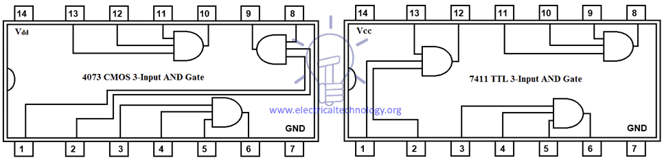
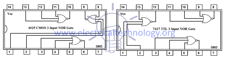
4025 CMOS and 7427 TTL 3-Input NOR Gate
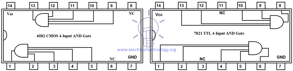
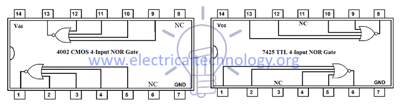
4002 CMOS and 7425 TTL 4-Input NOR Gate
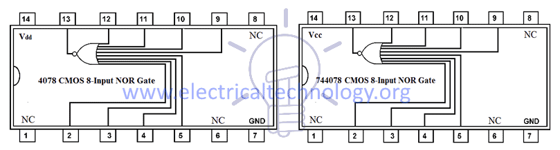
4078 CMOS and 744078 TTL 8-Input NOR Gate
Commonly available NOR Logic Gate IC are given in the table below:
| 4000 Dual 3 Input NOR Gate + 1 Inverter |
| 4001 Quad 2 Input NOR Gate |
| 4002 Dual 4 Input NOR Gate |
| 4025 Triple 3-Input NOR Gate |
| 4043 Quad NOR R/S Latch |
| 4078 8-Input OR Gate |
| 4572 Hex Gate, Quad NOT, Single NAND, Single NOR |
| 741G02 Single 2-Input NOR Drivers |
| 7403 Quad 2-Input NAND gate with open collector outputs |
| 7423 Expandable Dual 4-Inoput NOR Gate with strobe |
| 7425 Dual 4-Input NOR Gate with strobe |
| 7427 Triple 3 Input NOR Gate |
| 741G27 Single 3-Input NOR Gate |
| 7428 Quad 2-Input NOR Buffer |
| 7433 Quad 2-Input NOR Buffer with open collector outputs |
| 7436 Quad 2-Input NOR Gate (Different Pin out than 7402) |
| 74128 Quad 2-Input NOR line Driver |
| 74135 Quad Exclusive OR / NOR Gate |
| 74232 Quad NOR Schmitt Trigger |
| 74260 Dual 5-Input NOR Gate |
| 74805 Hex 2-Input NOR Drivers |
| 744002 Dual 4-Input NOR Gate |
| 744078 8-Input OR / NOR GATE |
NOR Gate Applications
Logic NOR Gate is a universal gate which can be used to construct other basic gates like AND gate. In real life, NOR gates are used in
- Cell phone
- Calculators
- Computing
- STB
- Digital Logic Circuits
- LCD TV
- Decision Making circuit like Mixer Tanks in the factory
- Industrial Controllers
You may also read more about Digital Logic gates
Logic NOT Gate – Digital Inverter Logic Gate Digital Logic OR Gate Digital Logic AND Gate Exclusive-NOR (XNOR) Digital Logic GateThe post Digital Logic NOR Gate – Universal Gate appeared first on Electrical Technology.
April 30, 2018 at 06:20AM by Department of EEE, ADBU: https://ift.tt/2AyIRVT