Vaaman is an RK3399-Powered SBC with Efinix Trion T120 FPGA

The Vaaman is an RK3399-powered SBC that also includes an Efinix Trion T120 FPGA onboard. The...

The post Vaaman is an RK3399-Powered SBC with Efinix Trion T120 FPGA appeared first on Electronics-Lab.com.


View more at https://www.electronics-lab.com/vaaman-is-an-rk3399-powered-sbc-with-efinix-trion-t120-fpga/.

Credit- ELECTRONICS-LAB. Distributed by Department of EEE, ADBU: https://tinyurl.com/eee-adbu
Curated by Jesif Ahmed

Reference Design For Software Configurable Pacemaker

This reference design revolutionises pacemaker detection in medical devices, offering precise control, seamless integration, and broad applicability in cardiac care technology.

The pacemaker is an essential medical device designed to regulate heartbeats in patients experiencing arrhythmias, such as tachycardia and bradycardia. This electronic device is surgically implanted just under the collarbone and consists of two main components: the pulse generator and the leads or electrodes. The pulse generator, which houses the battery and electrical circuits, generates electrical impulses that stimulate the heart muscles, ensuring regular contractions and a steady heartbeat. The leads connect the pulse generator to the heart’s right ventricle, enabling the transmission of electrical impulses throughout the heart.

Detecting the pacemaker’s electrical signals, or pace artifacts, can be challenging due to their small amplitude, narrow width, and varying slope, all compounded by background electrical noise. With the advancement in pacing therapy, a wide array of pacemaker modes is available, such as single-chamber and three-chamber pacing, each with its unique signal characteristics. Moreover, medical standards dictate specific conditions for pacemaker detection and the display of pacing artifacts.

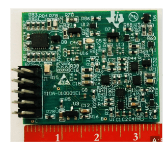
This reference design, TIDA-010005 by Texas Instruments (TI), introduces a compact hardware-based circuit for pacemaker pulse detection during electrocardiogram (ECG) measurements to address these challenges. It visually indicates a valid pace signal through an onboard LED. It allows users to configure various parameters of the pacing signal, including amplitude, rise time, pulse duration, and polarity, using software and an onboard digital-to-analog converter (DAC). The design incorporates an analog-to-digital converter (ADC) for reading measured values.

The key features of this design encompass a range of functionalities to enhance pacemaker detection in medical devices. Firstly, it includes programmable thresholds, accurately detecting varying rise times, amplitudes, durations, and polarities. Secondly, the design incorporates an I2C bus interface, providing access to measured parameters and the conditioned pace signal for further analysis and processing. Additionally, it is designed to be compatible with Texas Instruments’ ADS129X series of ECG front-end devices, ensuring seamless integration. The versatility of the design is evident in its ability to identify various types of pacemaker signals, making it suitable for a wide range of applications. Moreover, the compact size of the circuit, measuring just 29 mm × 35 mm, allows for easy implementation in various medical devices.

This reference design has potential applications in different medical devices, including ECG patches, electrocardiogram devices, multiparameter patches, and patient monitors with ECG modules or subsystems. By enhancing the accuracy of pacemaker detection, this design contributes significantly to advancing cardiac care technology, ensuring more reliable monitoring and treatment for patients with heart arrhythmias.

TI has tested this reference design. It comes with a Bill of Material (BOM), schematics, test reports, PCB layout, and Gerber files. The company’s website has additional data about the reference design. To read more about this reference design, click here.

The post Reference Design For Software Configurable Pacemaker appeared first on Electronics For You.


View more at https://www.electronicsforu.com/electronics-projects/reference-design-for-software-configurable-pacemaker.

Credit- EFY. Distributed by Department of EEE, ADBU: https://tinyurl.com/eee-adbu
Curated by Jesif Ahmed

Ultrafast Soft Recovery Diode Modules  Deliver High Reliability

  • The devices, featuring a common cathode configuration, can withstand IOL cycles up to five times that of the previous TO-244 generation. 
  • This enhancement improves the modules’ life expectancy while simultaneously reducing losses.

Vishay Intertechnology, Inc. have announced the release of two new FRED Pt 500 A Ultrafast soft recovery diode modules in the innovative TO-244 Gen III package. The new modules, VS-VSUD505CW60 and VS-VSUD510CW60, offer higher reliability compared to previous-generation solutions, aiming to reduce losses and EMI / RFI in high frequency power conditioning systems.

The rugged package of the diode modules can withstand 46,000 IOL cycles under specified conditions, providing an improved life expectancy over previous-generation devices. The industry-standard package is footprint-compatible with competing solutions in the package, allowing for a seamless drop-in replacement for existing designs.

Key Features of the Diode Modules are:

  • Ultrafast recovery
  • Designed for industrial level
  • UL approved file E222165

These diode modules are ideally suited for applications such as high frequency welding, high current converters, ballast water management systems (BWMS) in railway equipment, cranes, and ships, UPS, and other applications where switching losses contribute significantly to the total losses. The softness of their recovery eliminates the need for a snubber in these applications, reducing component counts and lowering costs. Offered in a common cathode configuration, the diode modules provide low forward voltage drop down to 0.82 V, thermal resistance — junction to case — of 0.16 °C/W, and an operating temperature range up to +175 °C. Samples and production quantities of the new FRED Pt soft recovery diode modules are available now, with lead times of 26 weeks.

The post Ultrafast Soft Recovery Diode Modules  Deliver High Reliability appeared first on Electronics For You.


View more at https://www.electronicsforu.com/news/ultrafast-soft-recovery-diode-modules-deliver-high-reliability.

Credit- EFY. Distributed by Department of EEE, ADBU: https://tinyurl.com/eee-adbu
Curated by Jesif Ahmed

Solar-Powered Emission-Free Tech Turns Saltwater Into Drinking Water

This solar-powered system converts salt water into fresh drinking water and presents a cost-effective solution for rural areas, promising to address waterborne diseases and enhance agricultural sustainability.

Water stress affects approximately a quarter of the global population, with 1.6 billion people in rural areas facing water scarcity. In India, where 60% of land has saline water, efficient desalination methods are urgently needed. Traditional desalination technologies often rely on costly batteries or unreliable grid systems, limiting their accessibility in developing countries.

Scientists have unveiled a solar-powered system designed to convert saltwater into fresh drinking water, potentially reducing waterborne diseases like cholera. This new system,offers a more than 20% cost reduction compared to traditional methods and is suitable for deployment in rural areas worldwide. The technology, developed by researchers from King’s College London in collaboration with MIT and the Helmholtz Institute for Renewable Energy Systems, builds upon existing processes for converting saline groundwater to freshwater. By utilizing specialized membranes to separate salt ions from water, the system ensures consistent freshwater production using solar energy.

A key feature of the system is its adaptability to variable sunlight conditions, achieved by adjusting voltage and saltwater flow rates. Testing conducted in rural communities, such as Chelleru in India and replicated conditions in New Mexico, demonstrated the system’s capability to produce up to 10 m3 of fresh drinking water per day, enough for 3,000 people. The team emphasized the potential benefits for rural communities, citing increased water supply and associated health improvements. The system’s ability to operate off-grid offers a sustainable, cost-effective alternative for communities facing water scarcity and contamination. They highlighted the system’s affordability and sustainability, noting its potential for use beyond developing areas, including agriculture. The team plans to scale up the technology’s availability in India through local partnerships and establish a startup with MIT to commercialize the technology.

The system’s application in wastewater treatment and ocean alkalinity enhancement for CO2 absorption demonstrates its broader environmental and climate benefits. By providing a low-cost, energy-efficient solution, the technology has the potential to transform water access and agricultural practices, contributing to global sustainability efforts.

The post Solar-Powered Emission-Free Tech Turns Saltwater Into Drinking Water appeared first on Electronics For You.


View more at https://www.electronicsforu.com/news/solar-powered-emission-free-tech-turns-saltwater-into-drinking-water.

Credit- EFY. Distributed by Department of EEE, ADBU: https://tinyurl.com/eee-adbu
Curated by Jesif Ahmed

Industry Leading Low On Resistance 80 V MOSFET For Automotive

The MOSFET features low package resistance, inductance, and a high avalanche current capability, making it highly suitable for automotive applications.

Infineon Technologies has unveiled the IAUCN08S7N013, the inaugural product in its innovative OptiMOS 7 80 V power MOSFET series. This advanced technology MOSFET is engineered for exceptional power density and is housed in the versatile, durable, and high-current SSO8 5 x 6 mm² SMD package. The series is ideally suited for emerging 48 V board net applications and is tailored for the rigorous demands of automotive applications, including electric vehicle (EV) DC-DC converters, 48 V motor control for systems such as electric power steering (EPS), 48 V battery switches, and electric two- and three-wheelers. 

The key features include:

  • RDS(on) reduced > 50% from prior best
  • Industry’s best RDS(on)
  • Industry’s best FOM (RDS(on) x Qg)
  • Fast switching times (turn on/off)
  • Low package resistance and inductance
  • High avalanche current capability
  • High SOA ruggedness
  • Excellent thermal performance
  • Extended qualification beyond AEC-Q101
  • Enhanced electrical testing
  • MSL1 up to 260°C peak reflow
  • 175°C operating temperature

It has a more than 50 per cent reduction in RDS(on) compared to its predecessor, achieving an industry-leading maximum of 1.3 mΩ. This improvement results in minimized conduction losses, superior switching performance, and unparalleled power density in a compact 5 x 6 mm² package. It also surpasses the AEC-Q101 standard with an extended qualification for enhanced reliability and performance in demanding automotive environments.

Its design maximises power density while maintaining a small footprint, allowing for efficient cooling. The increased design ruggedness and focus on automotive robustness make it ideal for demanding applications. High-quality production standards for automotive use further enhance its reliability and performance. It has many potential applications, particularly in the automotive sector. It can be used in high-voltage to 48V DC-DC converters in electric vehicles, various 48V systems, and DC-DC converters for 48V to 12V and 48V to 24V conversions.

Its versatility extends to 48V motor control applications such as electric power steering (EPS), braking, suspension, HVAC, and eTurbo systems, as well as 48V heating solutions like catalyst/eCAT, PTC heaters, and windscreen de-icing. The MOSFET is also suitable for other 48V auxiliary loads, 48V pumps and fans, 48V power distribution, and 48V battery management systems (BMS) and battery disconnect. Furthermore, it can be utilized in light electric vehicles, such as 2 and 3 wheelers, for traction inverters and chargers.

The post Industry Leading Low On Resistance 80 V MOSFET For Automotive appeared first on Electronics For You.


View more at https://www.electronicsforu.com/news/industry-leading-low-on-resistance-80-v-mosfet-for-automotive.

Credit- EFY. Distributed by Department of EEE, ADBU: https://tinyurl.com/eee-adbu
Curated by Jesif Ahmed

Connectors For Better Data And Power Transfer

The new range of connectors is designed for devices, offering durability and placement for data and power transfer.

Connectors

Harwin has introduced a new range of board-to-board connectors called the Flecto family, designed for high-performance applications requiring data and power transfer. These connectors can handle small movements in multiple directions, making them suitable for high-speed automated assembly and increasing their resistance to shock and vibration.

The Flecto connectors offer up to 160 contacts in a symmetrical double-row layout and come in three miniature pitch sizes: 0.5mm, 0.635mm, and 0.8mm. They can accommodate up to ±0.5 mm movement in both the X and Y axes, allowing for precise placement of multiple connectors between two PCBs, even with slight misalignments.

Additionally, the flexibility in positional tolerance of the connectors helps maintain connection integrity during shock and vibration events, reducing the risk of degradation or failure due to fretting, which happens when long-term vibration wears away the plating on rigid mating pins, exposing the underlying alloy to oxidation.

The connectors accommodate board-to-board mating heights starting from 7.2mm and support data rates up to 12 Gbit/s. The 0.5mm pitch variants come with additional power pins capable of handling currents up to 3A. These connectors are designed for vertical and horizontal configurations, allowing for parallel or perpendicular connections. Flecto signal-only connectors are equipped with location pegs or posts to prevent movement during soldering. In contrast, mixed-signal and power connectors have solderable posts through the board for precise positioning and increased strength. Some connectors have shrouded contacts to protect against damage when not connected, and others are polarized to ensure correct mating orientation.

The range is suitable for various applications, including factory automation, electric vehicles, LED displays, security cameras, IoT devices, data communications, and embedded systems.

“Growing demand for multiple connectors per board pair increases the potential for mechanical alignment issues due to the capabilities of automatic pick-and-place systems and the associated reflow process, which can cause connectors to experience unintended strain,” says Ryan Smart, Harwin’s Vice President of Product. 

The post Connectors For Better Data And Power Transfer appeared first on Electronics For You.


View more at https://www.electronicsforu.com/news/connectors-for-better-data-and-power-transfer.

Credit- EFY. Distributed by Department of EEE, ADBU: https://tinyurl.com/eee-adbu
Curated by Jesif Ahmed

Single Cylinder ECU Reference Design

Explore the key features, including wide voltage operation, robust protection mechanisms, and direct MCU interfacing, that make this reference design a comprehensive solution for single-cylinder engine control.

The Small Engine Reference Design is a compact hardware solution that controls single-cylinder engines. It is based on a combination of the company’s semiconductor components, including the MC9S12P128 microcontroller, the MC33812 Small Engine Integrated Circuit, and the MC33880 Configurable Octal Serial Switch. A 12 V battery powers this unit and can control various engine loads such as fuel injectors, inductive ignition coils, relays, incandescent lamps, and LEDs.

Regarding inputs, the Engine Control Unit (ECU) accepts signals from switches and sensors, including an Engine Stop switch, manifold air pressure sensor, engine temperature sensor, and variable reluctance sensors. The application software that runs on this unit contains the engine control strategy, which is crucial for the engine’s proper functioning. Although this reference design is not intended for production purposes specific to any engine, it aims to provide a look and feel similar to that of a production module. Its compact size, resembling that of a business card, and its minimal provision for expansion are notable features.

This reference design, KIT33812ECUEVME by NXP, is a fully functional single-cylinder engine control unit equipped with various key features to ensure reliable and efficient operation. It supports the company’s 33812 and 9S12P128 MCU devices and can be configured for dual-cylinder engines, although it requires the application to tolerate simultaneous sparks in both cylinders. The unit operates over a wide voltage range of approximately 4.7 V to 36 V. It includes a fuel injector driver with a typical current limit of 4.0 A, an ignition pre-driver that can drive IGBT or Darlington bipolar junction transistors, and relay and lamp drivers with current limits of 4.0 A and 1.5 A, respectively. 

The external outputs are protected against short-circuiting to the battery and over-current to ensure safety and durability. In contrast, the ignition and other drivers are protected against over-temperature conditions. The unit directly interfaces with the MCU using a 5.0 V parallel interface and features a VCC voltage pre-regulator that provides +5.0 V power for the MCU. Additional functionalities include an MCU Power On RESET generator, an MCU watchdog timer circuit, and independent fault annunciation outputs for ignition and injection. For debugging purposes and communicating diagnostic messages, the design incorporates an ISO-9141 K-Line transceiver. Overall, this reference design offers a comprehensive solution for controlling single-cylinder engines, with a range of features and protections to ensure efficient and reliable operation.

NXP has tested this reference design, which comes with a bill of materials (BOM), schematics, and other data. The company’s website has additional data about the reference design. To read more about this reference design, click here.

The post Single Cylinder ECU Reference Design appeared first on Electronics For You.


View more at https://www.electronicsforu.com/electronics-projects/single-cylinder-ecu-reference-design.

Credit- EFY. Distributed by Department of EEE, ADBU: https://tinyurl.com/eee-adbu
Curated by Jesif Ahmed

Axiomtek’s CEM320 Delivers Optimized Processing and Graphics Performance with Low Power Consumption

Axiomtek – a world-renowned leader relentlessly devoted to the research, development, and manufacture of a series...

The post Axiomtek’s CEM320 Delivers Optimized Processing and Graphics Performance with Low Power Consumption appeared first on Electronics-Lab.com.


View more at https://www.electronics-lab.com/axiomteks-cem320-delivers-optimized-processing-and-graphics-performance-with-low-power-consumption/.

Credit- ELECTRONICS-LAB. Distributed by Department of EEE, ADBU: https://tinyurl.com/eee-adbu
Curated by Jesif Ahmed

JOB: Trouble Shooting Technician At Sercomm In Chennai

APPLY HERE ON LINKEDIN

Location: Chennai

Company: Sercomm

Job Description

As a Troubleshooting Technician, you will be responsible for troubleshooting and resolving complex issues related to printed circuit board assemblies (PCBA).

Responsibilities

  • Troubleshoot and debug PCBA assemblies to identify and resolve hardware and software issues
  • Utilize oscilloscopes, multimeters, and other electronic test equipment to perform detailed analysis for fault identification
  • Collaborate with engineers and designers to develop effective debug strategies
  • Perform component-level diagnostics and repair faulty circuitry
  • Develop and maintain test plans and procedures for PCBA assemblies
  • Document and communicate test results, findings, and recommendations to cross-functional teams
  • Conduct root cause analysis to identify recurring issues and implement corrective measures
  • Ensure compliance with quality standards and regulatory requirements
  • Maintain a clean and organized work area
  • Maintain and calibrate electronic testing equipment to ensure accuracy and reliability.
  • Stay updated with industry trends, advancements, and best practices in debugging techniques.

Requirements

  • Associate degree or certification in Electrical/Electronic Engineering or a related field.
  • Proven experience as a Debug Technician or in a similar role.
  • Strong knowledge of electrical and electronic components, circuitry, and systems.
  • Proficient in using diagnostic tools, oscilloscopes, multimeters, and other relevant equipment.
  • Excellent problem-solving skills with the ability to think critically and analytically.
  • Strong attention to detail and an ability to work effectively in a fast-paced environment.
  • Effective communication skills and ability to collaborate with cross-functional teams.

The post JOB: Trouble Shooting Technician At Sercomm In Chennai appeared first on Electronics For You.


View more at https://www.electronicsforu.com/career/trouble-shooting-technician-sercomm-chennai.

Credit- EFY. Distributed by Department of EEE, ADBU: https://tinyurl.com/eee-adbu
Curated by Jesif Ahmed

Wireless Power Transmitter Reference Design

The reference design supports Qi 2.0 with a dual-pad wireless power transmitter, offering flexibility and security across various applications.

Wireless power transmitter

Wireless power transmitters are increasingly crucial in today’s technology-driven world due to their convenience and ability to eliminate the need for physical cables and connectors. This improves the aesthetic appeal of spaces by reducing clutter and enhances the durability of devices by minimizing wear and tear on physical connectors. Furthermore, wireless charging offers safety advantages by reducing the risk of electric shock and short circuits. The integration of wireless charging technology into a wide range of devices, from smartphones to electric vehicles, is a testament to its innovative potential. Standardized protocols like Qi ensure compatibility across different devices, making wireless charging more accessible and convenient for users. Overall, the need for wireless power transmitters is driven by their ability to provide a seamless, safe, and efficient charging experience, which is becoming increasingly important in our daily lives.

The reference design of Qi 2.0 dual-pad wireless power transmitter by Microchip features a dual-pad multi-coil wireless power transmitter controlled by a single dsPIC33 Digital Signal Controller (DSC), supporting both Extended Power Profile (EPP) and Magnetic Power Profile (MPP) of Qi 2.0. The DSC’s flexible software architecture allows optimized software to manage a combination of EPP and MPP with one controller. As an automotive-grade reference design, it includes CryptoAuthentication™ 
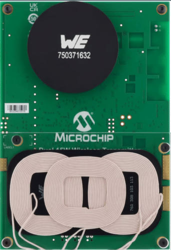
to meet the security requirements of the standard. The design comprises the dsPIC33 DSC, the Trust Anchor TA100/TA010 secure storage subsystem provisioned as a licensed Wireless Power Consortium (WPC) Manufacturer Certificate Authority (CA), and other components depicted in the block diagram. We provide design files and software source code under the appropriate terms and conditions for a seamless design process and first-pass success.

The reference design primarily aims at electronics designers and manufacturers developing wireless charging solutions. This design is especially suitable for automotive applications, given its automotive-grade robustness and security features. It finds applications across various sectors, including consumer electronics for charging smartphones and other personal devices and the automotive industry for in-vehicle charging pads. These medical devices require sterilization or have limited power access, industrial settings for charging devices in hazardous environments, and furniture or infrastructure for seamless integration into tables and desks for convenient charging.

This system’s dual-pad design adheres to the WPC Qi 2.0 standard, incorporating both Magnetic Power Profile (MPP) and Extended Power Profile (EPP). A single dsPIC33 microcontroller manages both charging pads simultaneously. This automotive-grade reference design also supports proprietary fast charging. Its programmable software-based solution allows a mix of MPP/MPAx transmitter types across the two pads. Additionally, this programmable approach facilitates the customization and optimization of Magnetic Power Alignment (MPLA) and Q-factor-based Foreign Object Detection (Q-FOD) tuning.

Microchip has tested this reference design. It comes with a bill of materials (BOM), schematics, etc. You can find additional data about the reference design on the company’s website. To read more about this reference design, click here.

The post Wireless Power Transmitter Reference Design appeared first on Electronics For You.


View more at https://www.electronicsforu.com/electronics-projects/wireless-power-transmitter-reference-design.

Credit- EFY. Distributed by Department of EEE, ADBU: https://tinyurl.com/eee-adbu
Curated by Jesif Ahmed

Smarter Robots Learn To Adapt and Complete Tasks

MIT researchers are teaching robots to adapt using language models, enabling them to handle unexpected situations and complete tasks.

In this collaged image, a robotic hand tries to scoop up red marbles and put them into another bowl while a researcher’s hand frequently disrupts it. The robot eventually succeeds. Credits:Image: Jose-Luis Olivares, MIT. Stills courtesy of the researchers
In this collaged image, a robotic hand tries to scoop up red marbles and put them into another bowl while a researcher’s hand frequently disrupts it. The robot eventually succeeds.
Credits:Image: Jose-Luis Olivares, MIT. Stills courtesy of the researchers

Robots are being trained to perform increasingly complex household tasks, from wiping up spills to serving food, often through imitation, where they are programmed to copy motions guided by a human. While robots are excellent mimics, they may only know how to handle unexpected bumps and nudges if engineers program them to adjust accordingly, which could result in them having to restart their tasks from the beginning.

MIT engineers have integrated robot motion data with large language models (LLMs) to give robots common sense for off-path situations. This enables robots to break down tasks into subtasks and adjust to disruptions without restarting or needing explicit programming for every potential failure.

Language task

The researchers demonstrated a marble-scooping task involving a sequence of subtasks like reaching, scooping, and pouring. Without specific programming for each subtask, a robot nudged off course would have to restart. They explored using LLMs, which can process text to generate logical lists of subtasks, like “reach,” “scoop,” and “pour.” This approach could enable robots to self-correct in real time without extensive additional programming.

Mapping marbles

The team developed an algorithm to connect a robot’s physical position or image state with a subtask’s natural language label, known as “grounding.” This algorithm learns to automatically identify the robot’s semantic subtask, such as “reach” or “scoop,” based on its physical coordinates or image view. In experiments with a robotic arm trained on a marble-scooping task, the team demonstrated this approach by guiding the robot through the task and using a pre-trained LLM to list the steps involved.

The team then allowed the robot to carry out the scooping task using the newly learned grounding classifiers. As the robot progressed, experimenters pushed and nudged it off its path and knocked marbles off its spoon. Instead of stopping and starting over or continuing unquestioningly, the robot could self-correct and complete each subtask before moving on to the next.

The post Smarter Robots Learn To Adapt and Complete Tasks appeared first on Electronics For You.


View more at https://www.electronicsforu.com/news/smarter-robots-learn-to-adapt-and-complete-tasks.

Credit- EFY. Distributed by Department of EEE, ADBU: https://tinyurl.com/eee-adbu
Curated by Jesif Ahmed

JOB: Design Engineering Architech At Cadence In Bengaluru and Noida

APPLY HERE

Location: Bengaluru and Noida

Company: Cadence

  • Design and implement DFT IP w/ Verilog/SystemVerilog and/or VHDL
  • Design and implement RTL for DFT IP incl. POST, IST
  • Develop synthesis automation for DFT IP including synthesis and timing constraints, RTL insertion and verification
  • Own and maintain, extend, and enhance existing DFT IP like LBIST

The post JOB: Design Engineering Architech At Cadence In Bengaluru and Noida appeared first on Electronics For You.


View more at https://www.electronicsforu.com/career/design-engineering-architech-cadence-bengaluru-noida.

Credit- EFY. Distributed by Department of EEE, ADBU: https://tinyurl.com/eee-adbu
Curated by Jesif Ahmed

JOB: Customer Engineer Existing Installation – FACT At Schindler In Ahmedabad

APPLY HERE

Location: Ahmedabad

Company: Schindler

Your Responsibilities

The Service Engineer creates operational added value through the performance of maintenance, repairs and small modernizations on customer’s equipment in an efficient, effective and professional manner in order to provide outstanding customer service following the safety rules.

Key responsibilities include:

  • Take responsibility for the assigned service route and organize his time to complete the assigned visits and the specific tasks within each visit in order to maximize the safety and reliability of the equipment.
  • Respond to all call backs that are assigned in a timely manner and be available for call-back coverage during regular work hours, nights, weekends and holidays.
  • Perform all service, repairs and small modernizations according to the Schindler standards, including safety policies.
  • Keep the customer informed regarding the condition of his equipment, preventive and corrective repairs and discretionary repairs or modernizations.
  • Complete all required data inputs in a diligent and honest fashion; these include time reporting, parts usage, call-back reporting, maintenance performance and repair and modernization work reports in Field Link.

Expertise: Desired experience as a Technician in E&E industry for at least four years (ITI) and two years for Diploma holder.

Knowledge and Skills: Desired knowledge in electronics, electricity, mechanics and hydraulics. Customer-oriented behavior, Communication Skills

Education: Diploma in Engineering (Electrical or Electronics)

The post JOB: Customer Engineer Existing Installation – FACT At Schindler In Ahmedabad appeared first on Electronics For You.


View more at https://www.electronicsforu.com/career/customer-engineer-existing-installation-fact-schindler-ahmedabad.

Credit- EFY. Distributed by Department of EEE, ADBU: https://tinyurl.com/eee-adbu
Curated by Jesif Ahmed

Circuit breaker schematics in a nutshell: Tripping, closing and blocking coil arrangements

This technical article embarks on a comprehensive exploration of various facets of circuit breaker technology, traversing from the fundamental principles of solenoid coils to the sophisticated mechanisms of SF6 density... Read more

The post Circuit breaker schematics in a nutshell: Tripping, closing and blocking coil arrangements appeared first on EEP - Electrical Engineering Portal.


View more at: https://electrical-engineering-portal.com/circuit-breaker-schematics-tripping-closing-blocking-coil-arrangements Credit- EEE - Electrical Engineering Portal. Distributed by Department of EEE, ADBU: https://tinyurl.com/eee-adbu
Curated by Jesif Ahmed.

Circuit breaker schematics in a nutshell: Tripping, closing and blocking coil arrangements

This technical article embarks on a comprehensive exploration of various facets of circuit breaker technology, traversing from the fundamental principles of solenoid coils to the sophisticated mechanisms of SF6 density... Read more


The post Circuit breaker schematics in a nutshell: Tripping, closing and blocking coil arrangements appeared first on EEP - Electrical Engineering Portal. Credit: EEP- Electrical Engineering Portal. Visit:


http://dlvr.it/T4ZJCx

From Idea to Chip Design in Minutes – With Tiny Tapeout 6 You Can Design your Custom Silicon for Just $300

With Tiny Tapeout 6, you can design your custom ICs, get them fabricated, and then receive...

The post From Idea to Chip Design in Minutes – With Tiny Tapeout 6 You Can Design your Custom Silicon for Just $300 appeared first on Electronics-Lab.com.


View more at https://www.electronics-lab.com/from-idea-to-chip-design-in-minutes-with-tiny-tapeout-6-you-can-design-your-custom-silicon-for-just-300/.

Credit- ELECTRONICS-LAB. Distributed by Department of EEE, ADBU: https://tinyurl.com/eee-adbu
Curated by Jesif Ahmed

Industrial OpenWrt gateway features MediaTek MT7628 SoC, WiFi, LTE, and GNSS connectivity

Atreyo AG-702 industrial OpenWrt gateway

The Atreyo AG-702 is an industrial OpenWrt gateway powered by the MediaTek MT7628 processor, featuring dual...

The post Industrial OpenWrt gateway features MediaTek MT7628 SoC, WiFi, LTE, and GNSS connectivity appeared first on Electronics-Lab.com.


View more at https://www.electronics-lab.com/industrial-openwrt-gateway-features-mediatek-mt7628-soc-wifi-lte-and-gnss-connectivity/.

Credit- ELECTRONICS-LAB. Distributed by Department of EEE, ADBU: https://tinyurl.com/eee-adbu
Curated by Jesif Ahmed

Revolutionizing Wireless Connectivity: Exploring the Compex WLE7002E25 WiFi 7 Mini PCIe Module

The Compex WLE7002E25 is a WiFi 7 module designed in a standard mini PCIe form factor,...

The post Revolutionizing Wireless Connectivity: Exploring the Compex WLE7002E25 WiFi 7 Mini PCIe Module appeared first on Electronics-Lab.com.


View more at https://www.electronics-lab.com/revolutionizing-wireless-connectivity-exploring-the-compex-wle7002e25-wifi-7-mini-pcie-module/.

Credit- ELECTRONICS-LAB. Distributed by Department of EEE, ADBU: https://tinyurl.com/eee-adbu
Curated by Jesif Ahmed

Exploring the Security and Performance Features of nRF9151: A Breakdown of Arm Cortex-M33, TrustZone, and CryptoCell

The newly developed System-in-Package (SIP) is a significant advancement for power-efficient cellular projects. It features a...

The post Exploring the Security and Performance Features of nRF9151: A Breakdown of Arm Cortex-M33, TrustZone, and CryptoCell appeared first on Electronics-Lab.com.


View more at https://www.electronics-lab.com/exploring-the-security-and-performance-features-of-nrf9151-a-breakdown-of-arm-cortex-m33-trustzone-and-cryptocell/.

Credit- ELECTRONICS-LAB. Distributed by Department of EEE, ADBU: https://tinyurl.com/eee-adbu
Curated by Jesif Ahmed

Live DIY: How To Make A Digital Thermometer

Key Takeaways

  • What is a digital thermometer?    
  • How we interface LM35 and Arduino Uno to the thermometer    
  • How to install this project of  Thermometer.    
  • How this digital thermometer works    
  • What is the use of this digital thermometer    
  • Brief introduction of LM35 temperature sensor    
  • What is the purpose of using LM35 in this project?

Who should Attend

  • DiYer and Electronics Enthusiast    
  • Researchers and students working on electronics project    
  • Students studying engineering /diploma    
  • Thermometer designer    
  • Hobbyist    
  • Thermometer Manufacturer

The post Live DIY: How To Make A Digital Thermometer appeared first on Electronics For You.


View more at https://www.electronicsforu.com/videos-slideshows/live-diy-make-digital-thermometer.

Credit- EFY. Distributed by Department of EEE, ADBU: https://tinyurl.com/eee-adbu
Curated by Jesif Ahmed

Brain-Inspired Chip For Wireless Data Gathering With Salt-Sized Sensors

With their energy-efficient design and scalability, these microsensors hold immense potential for advancing healthcare and environmental monitoring.

The team led by Brown University engineers has developed tiny microelectronic chips that could revolutionize wireless communication networks. These chips are no larger than a grain of salt and can efficiently transmit, receive, and decode data in real-time. This paves the way for their integration into wearable devices or implantation in the human body.

The silicon sensors within these chips are designed to mimic the way neurons in the brain communicate through spikes of electrical activity. By detecting specific events and transmitting data as short bursts of electrical spikes, these sensors conserve energy and bandwidth. “The sensors would not be sending out data all the time—they’d just be sending relevant data as needed,” explained Jihun Lee, a postdoctoral researcher at Brown and the study’s lead author. One key advantage of this system is its scalability. Traditional sensor communication networks require perfect synchronization, which can be challenging to achieve. However, the novel radiofrequency transmission scheme used in this study allows each sensor to operate independently, avoiding the need for coordination with a central receiver.

The potential applications of this technology are vast, particularly in the field of biomedical sensors. “The most demanding environment for these sensors will always be inside the human body,” said Arto Nurmikko, a professor in Brown’s School of Engineering and the study’s senior author. The development of these microsensors could lead to advancements in monitoring physiological activity across various areas of interest in medicine. These sensors also stand out for their energy efficiency. External transceivers supply wireless power to the sensors as they transmit data, eliminating the need for a direct power source or battery. This feature makes them versatile for use in different environments.

The research builds on previous work from Nurmikko’s lab, which introduced a neural interface system called “neurograins.” The current study demonstrates the system’s efficiency and potential for scalability, with successful lab tests involving 78 sensors and simulations showing the possibility of decoding data from around 8,000 hypothetically implanted sensors in primate brains. The team aims to optimize the system for reduced power consumption and explore broader applications beyond neurotechnology. This breakthrough marks a significant step forward in the development of wireless microsensor technology, with implications for various fields, including healthcare and environmental monitoring.

The post Brain-Inspired Chip For Wireless Data Gathering With Salt-Sized Sensors appeared first on Electronics For You.


View more at https://www.electronicsforu.com/news/brain-inspired-chip-for-wireless-data-gathering-with-salt-sized-sensors.

Credit- EFY. Distributed by Department of EEE, ADBU: https://tinyurl.com/eee-adbu
Curated by Jesif Ahmed

First Smart LiDAR For The Security Industry

The 3D LiDAR sensor features zone monitoring, object detection, and low false alarm rates for security applications.

LiDAR

Blickfeld introduces the “Blickfeld QbProtect,” a 3D LiDAR sensor for security applications. It features software for monitoring zones, fences, and facades, directly processing data on unauthorized entry on the device without additional computers. The sensor detects objects in various weather and lighting conditions, ensuring low false alarm rates and enhanced security. Installation is straightforward, and it integrates easily into standard security systems with configuration through a graphical interface.

The 3D LiDAR sensor is designed for security professionals, system integrators, and property managers who require advanced surveillance solutions. It is suitable for use in various settings, including commercial properties, industrial sites, and public spaces, where reliable perimeter monitoring and intrusion detection are critical.

The technology scans the environment with laser pulses, creating 3D point clouds. Users can define and adjust security zones in a 3D viewer within a browser-based interface, setting object size thresholds for alarm triggers. This minimizes false alarms by excluding small animals or vegetation. Data is anonymous, ensuring compliance with privacy regulations.

Alarm logic is customizable via the web interface, with drag-and-drop functionality. Users can apply presets for triggers and modify conditions as needed, allowing for a customized security solution without programming effort.

Setting up Blickfeld QbProtect is easy. It requires fewer cables since no external computer is needed for data analysis, thanks to its on-device software. Both data and power are transmitted over the same cable (Power over Ethernet). Built on Blickfeld’s Smart LiDAR “Qb2,” the hardware has a design with no rotating parts. Its housing is IP67-rated, protecting against dust and water, making the Blickfeld QbProtect robust, durable, and low maintenance.

Florian Petit, co-founder and CXO at Blickfeld, comments: “The new sensor is straightforward to operate through an integrated web GUI, setting new standards for user-friendliness. Security personnel immediately benefit from significantly improved, anonymous, and highly accurate detection of unauthorized entry into sensitive areas, such as power plants, airports, or other critical infrastructures.”

For more information, click here.

The post First Smart LiDAR For The Security Industry appeared first on Electronics For You.


View more at https://www.electronicsforu.com/special/first-smart-lidar-for-the-security-industry.

Credit- EFY. Distributed by Department of EEE, ADBU: https://tinyurl.com/eee-adbu
Curated by Jesif Ahmed

World’s Most Advanced 5G Modem-RF System

The modem-to-antenna system has a dedicated 5G AI Processor, 6-antenna architecture, and advanced features for various applications and industries.

X80

Since its inception, Qualcomm Technologies, Inc. has led the way in 5G technology and continues to drive innovation by introducing the Snapdragon X80 5G Modem-RF System. This solution is the latest in its series of modem-to-antenna systems and includes a dedicated 5G AI Processor and an architecture for 5G Advanced. The Snapdragon X80 introduces new industry features with its integrated NB-NTN satellite communications support, 6-antenna smartphone architecture, 6X carrier aggregation, and AI range extension for fixed wireless access customer premise equipment (CPE).

The Modem-RF System is designed for a broad range of users and applications, including smartphone manufacturers seeking to enhance connectivity and performance, mobile broadband providers aiming to deliver high-speed 5G connectivity, PC manufacturers looking to integrate 5G into laptops for seamless internet access, XR device makers creating immersive virtual and augmented reality experiences, the automotive industry for connected vehicle features, industrial IoT for remote monitoring and automation, private network operators for secure and high-speed connectivity, and fixed wireless access providers aiming to deliver broadband without wired connections.

Equipped with groundbreaking AI advancements powered by a dedicated tensor accelerator, the Snapdragon X80 enhances data speeds, reduces latency, and improves quality of service (QoS), coverage, location accuracy, spectrum efficiency, power efficiency, and multi-antenna management.

“The Snapdragon X80 modem-RF system sets the stage for 5G Advanced and the era of intelligent computing everywhere,” said Durga Malladi, senior vice president and general manager of technology planning and edge solutions at Qualcomm Technologies, Inc. “Leveraging AI is critical to the future of connectivity, this latest milestone underscores Qualcomm Technologies’ leadership at the intersection of cutting-edge AI and advanced modem-RF technology. The Snapdragon X80 5G Modem-RF System empowers OEMs and operators to create next-generation devices supporting 5G Advanced, with unrivalled capabilities and leading performance.”

For more information, click here.

The post World’s Most Advanced 5G Modem-RF System appeared first on Electronics For You.


View more at https://www.electronicsforu.com/special/worlds-most-advanced-5g-modem-rf-system.

Credit- EFY. Distributed by Department of EEE, ADBU: https://tinyurl.com/eee-adbu
Curated by Jesif Ahmed

JOB: PCB Engineer At UST In Bengaluru

APPLY HERE

Location: Bengaluru

Company: UST

Experience: 3-5 yrs.

Location: Bengaluru

Experience in Carrying out electrical simulations to optimize the design of new as well as of existing packages & PCBs.

Provisioning of electrical models, Analyzing customer-specific applications on package and system level Pre-silicon evaluating and optimization of the electrical performance of packages & PCBs.

Experience in package modelling (SPICE, IBIS and S-parameters), electromagnetic simulation, signal and power integrity checks or circuit design.

The post JOB: PCB Engineer At UST In Bengaluru appeared first on Electronics For You.


View more at https://www.electronicsforu.com/career/job-pcb-engineer-ust-bengaluru.

Credit- EFY. Distributed by Department of EEE, ADBU: https://tinyurl.com/eee-adbu
Curated by Jesif Ahmed

World’s Smallest and Lowest Power UWB SoC

The ultra-wideband SoC enables indoor and outdoor positioning, low power consumption, and precise connectivity through integration into IoT devices.

UWB SoC

Shenzhen Jieyang Microelectronics Co., Ltd. has released the GT1500, an ultra-wideband (UWB) system-on-chip (SoC) for ranging, positioning, and wireless connectivity applications. The SoC is designed for indoor and outdoor ranging and positioning without relying on network infrastructure coverage. It provides wireless connections at configurable data rates, enabling applications in mobile phones, wearable devices, digital keys, and more across access control, smart payment, smart homes, and smart cities.

The SoC is known for its low power consumption and performance, with a wafer-level packaging size of 9 square millimetres, making it the smallest UWB SoC chip. It integrates RF, analogue, and baseband functions with four receiving channels and works with an embedded MCU for control and protocol processing, all within a single chip.

Suitable for wearables, tags, and IoT products, the SoC simplifies 3D AoA design, reduces peripheral components, and lowers BoM costs. Its design enhances signal reception and UWB performance while extending battery life in UWB tags compared to similar products.

Some of the key features of the UWB SoC include:

  • Ultra-thin wafer-level package: 49-pin, 3.2mm x 2.8mm x 0.6mm
  • 1T4R architecture: Single chip with one transmitter and four receivers
  • Integrated protocols and software for standalone operation
  • Supports ranging types: Unilateral, bilateral, bidirectional
  • Supports 2D/3D AoA and TDoA measurement
  • Frequency range: 4.0 – 9.0 GHz
  • Communication rates: 1.2 Mbps, 27.2 Mbps, 7.8 Mbps, 6.8 Mbps, 850 Kbps
  • Interfaces: SPI, I2C, UART, GPIO
  • Accuracy: ±3 cm for distance, ±3 degrees for angle
  • Power consumption: 125mW (receivers), 69mW (transmitter)

Certified by the FiRa Alliance and compliant with the Car Connectivity Consortium (CCC) Digital Key 3.0 standard, the product offers features such as wafer-level packaging, a 1T4R architecture, integrated protocols and software, and support for various ranging and AoA techniques. It operates in the 4.0 to 9.0 GHz frequency range and offers multiple communication rates and interfaces, with a distance measurement accuracy of ±3 cm and angle measurement accuracy of ±3 degrees.

For more information, click here.

The post World’s Smallest and Lowest Power UWB SoC appeared first on Electronics For You.


View more at https://www.electronicsforu.com/special/worlds-smallest-and-lowest-power-uwb-soc.

Credit- EFY. Distributed by Department of EEE, ADBU: https://tinyurl.com/eee-adbu
Curated by Jesif Ahmed

Analog Switches To Monitor & Protect 1.8 V Electronic Systems

The series of 4- and 8-channel analogue switches are designed for monitoring and protecting 1.8 V systems, suitable for automotive, consumer, and industrial applications.

Analog switches

Nexperia has launched a new series of 4- and 8-channel analogue switches, the NMUX1308 and NMUX1309, for monitoring and protecting 1.8 V electronic systems. These switches are designed for automotive, consumer, and industrial applications, including sensor monitoring, diagnostics, and computing. They are suitable for use in automotive sensor monitoring, domestic appliances, and other electronic systems requiring reliable protection.

Typically, analogue switches require extra voltage translators due to the inability of the control circuitry to operate at the power supply voltage level of the switch. However, the switches have control pins that function independently of their power supply voltage range, eliminating the need for additional level-shifting components and thus saving space on the board and reducing costs.

The company claims to offer several features in the series of switches to enhance system safety. The fail-safe logic allows control pins to be biased before the system powers up and to remain biased even after the system has powered down, removing the need for power sequencing between the analogue switch and the microcontroller unit (MCU). Additionally, a power-off protection feature enables analog pins to be biased before system power-up and to stay biased after system power-down, eliminating power sequencing restrictions for the analog switch and various power rails supporting analog signals and ADC circuitry further down the signal chain. The integration of both features in the series prevents back-powering of the supply rail through any pin of the analogue switch.

These devices also incorporate injection current control circuitry, limiting output voltage shifts on the active channel to less than 5 mV during an overvoltage event on disabled signal channels. This removes the necessity for external diode and resistor networks, thereby saving board space and reducing costs. The switches come in leaded and leadless options, including a leadless package that supports Automated Optical Inspection (AOI) for automotive applications.

For more information, click here.

The post Analog Switches To Monitor & Protect 1.8 V Electronic Systems appeared first on Electronics For You.


View more at https://www.electronicsforu.com/special/analog-switches-to-monitor-protect-1-8-v-electronic-systems.

Credit- EFY. Distributed by Department of EEE, ADBU: https://tinyurl.com/eee-adbu
Curated by Jesif Ahmed

Choosing the Right Diode – Types and Uses Explained for Beginners

From small LED drivers to rectifiers to Switch Mode Power Supplies (SMPS), the diode is a...

The post Choosing the Right Diode – Types and Uses Explained for Beginners appeared first on Electronics-Lab.com.


View more at https://www.electronics-lab.com/choosing-the-right-diode-types-and-uses-explained-for-beginners/.

Credit- ELECTRONICS-LAB. Distributed by Department of EEE, ADBU: https://tinyurl.com/eee-adbu
Curated by Jesif Ahmed

PoE Active-Clamp Forward Converter Reference Design

This design offers a comprehensive solution for powering devices through PoE technology, focusing on efficiency, reliability, and compliance with industry standards.

The active clamp forward converter has emerged as a pivotal technology in Power over Ethernet (PoE), particularly for powering devices (PD) . Its significance lies in efficiently converting electrical power from a source to a PoE-enabled device, ensuring a stable and reliable power supply. This technology is especially crucial in modern networking and communication infrastructures, where the demand for seamless connectivity and uninterrupted power is paramount. By leveraging the active clamp forward converter, businesses and individuals can deploy a wide array of PoE devices without the need for additional power sources, thereby simplifying installation, reducing cabling complexity, and enhancing overall system efficiency.

This reference design PMP21318 by Texas Instruments showcases a Type-4, Class 8, 71-W active clamp forward converter specifically tailored for powering devices (PD) through Power over Ethernet (PoE) technology. At the heart of this design is the TPS2373-4 PD controller, which is responsible for the crucial functions of the detection and classification of PDs. This controller plays a pivotal role in activating the UCC2897A pulse-width modulation (PWM) controller, thanks to its advanced start-up feature. It supports power levels compliant with the IEEE802.3bt Type-4 standard. This ensures the design can cater to the latest and most demanding PD requirements It incorporates an automatic maintain power signature (MPS) mechanism, which is essential for ensuring continuous power delivery and system reliability. 

The advanced start-up feature of the  controller is another highlight of this design. It allows for a smooth and efficient initiation of the power conversion process, which is critical for the overall performance and longevity of the system. Including synchronous rectifiers in the design significantly enhances its efficiency. These rectifiers reduce power losses during the conversion process, thereby improving the system’s overall energy efficiency. It offers various output voltage options with a minimum input voltage of 42.5V, a maximum of 57V, a nominal output voltage of 12V, and a maximum output current of 6A, delivering an output power of 72W. It features an isolated, forward-active clamp topology for improved efficiency in PoE applications. 

The design is particularly suitable for communications equipment like WLAN/Wi-Fi access points, ensuring reliable power for uninterrupted connectivity. It is applicable in the industrial sector for powering fixed wired IP cameras, providing efficient and reliable power for surveillance and security purposes. It is well-suited for various applications, particularly in communications and industrial settings, where efficient and reliable power delivery is a critical requirement.

TI has tested this reference design. It comes with a Bill of Material (BOM), schematics, test reports, PCB layout, Gerber files, and more. The company’s website has additional data about the reference design. To read more about this reference design, click here.

The post PoE Active-Clamp Forward Converter Reference Design appeared first on Electronics For You.


View more at https://www.electronicsforu.com/electronics-projects/poe-active-clamp-forward-converter-reference-design.

Credit- EFY. Distributed by Department of EEE, ADBU: https://tinyurl.com/eee-adbu
Curated by Jesif Ahmed

Industry-First 36GB HBM3E 12H DRAM

The industry’s first 12-stack HBM3E DRAM with 1,280 GB/s bandwidth and 36 GB capacity is revolutionising AI applications and high-performance computing.

DRAM

Samsung Electronics, a leader in memory technology, announced the development of the HBM3E 12H, the industry’s first 12-stack HBM3E DRAM and the highest-capacity HBM product.

The DRAM provides a bandwidth of up to 1,280 gigabytes per second (GB/s) and a 36 gigabytes (GB) capacity, improving both aspects by more than 50% compared to the 8-stack HBM3 8H. The HBM3E 12H uses thermal compression non-conductive film (TC NCF), ensuring that the 12-layer products maintain the exact height specification as the 8-layer ones to comply with HBM package standards. This technology is expected to offer advantages for higher stacks as the industry aims to address chip die warping associated with thinner die. Samsung has reduced the thickness of its NCF material, achieving a chip gap of seven micrometres (µm) while eliminating voids between layers. These improvements result in a more than 20% increase in vertical density compared to the HBM3 8H product.

Samsung’s TC NCF also enhances the thermal properties of the HBM by allowing bumps of varying sizes between the chips. Smaller bumps are used for signalling during the chip bonding process, while larger ones are placed in areas requiring heat dissipation. This approach also contributes to higher product yield.

As AI applications continue to proliferate, the product is poised to be a solution for future systems demanding more memory. Its performance and capacity will enable customers to manage their resources more flexibly and reduce the total cost of ownership (TCO) for data centres. In AI applications, using the HBM3E 12H, compared to the HBM3 8H, can increase the average speed of AI training by 34% and expand the number of simultaneous users of inference services by more than 11.5 times.

“The industry’s AI service providers are increasingly requiring HBM with higher capacity, and our new HBM3E 12H product has been designed to answer that need,” said Yongcheol Bae, Executive Vice President of Memory Product Planning at Samsung Electronics. 

For more information, click here.

The post Industry-First 36GB HBM3E 12H DRAM appeared first on Electronics For You.


View more at https://www.electronicsforu.com/special/industry-first-36gb-hbm3e-12h-dram.

Credit- EFY. Distributed by Department of EEE, ADBU: https://tinyurl.com/eee-adbu
Curated by Jesif Ahmed

Development Board For Wi-Fi & Bluetooth Projects

The development board, featuring Wi-Fi, Bluetooth, low power consumption, and interfaces, unleashes the potential for IoT projects.

ADIY board

The ADIY Ai WB2 12F dev-Kit is a development board designed for the Ai WB2 12F modules, which are Wi-Fi & Bluetooth modules developed by Shenzhen Ai Thinker Technology Co., Ltd. These modules are powered by a BL602 chip that serves as the core processor and supports Wi-Fi 802.11b/g/n protocol and BLE 5.0 protocol. The BL602 chip features a 32-bit RISC CPU with low power consumption, 276 KB RAM, and various peripheral interfaces such as SDIO, SPI, UART, VDC, IR remote, PWM, ADC, DAC, PIR, and GPIO. This makes it suitable for various applications in the Internet of Things (IoT), mobile devices, wearable electronic devices, smart homes, and other fields.

The development board can be used by IoT developers, hardware engineers, and hobbyists working on projects that require Wi-Fi and Bluetooth connectivity. They also seem suitable for educational institutions teaching electronics and computer science. Additionally, startups creating innovative smart devices and wearable technology can benefit from the kit’s features.

The dev-Kit supports the IEEE 802.11 b/g/n protocol for Wi-Fi connectivity and various security protocols, including WPS, WEP, WPA, WPA2 Personal, WPA2 Enterprise, and WPA3. It operates on a 20MHz bandwidth with a maximum speed of 72.2 Mbps. For Bluetooth connectivity, it supports BLE 5.0 and Bluetooth Mesh, with multiple operating modes, including Station + BLE mode and Station + Soft AP + BLE mode.

For added security, it features a real random number generator (TRNG) and a public key accelerator (PKA) that supports large numbers of basic operations, with software providing application interfaces such as signature and verification.

It supports multiple sleep modes for power management with a deep sleep current of 12μA. It also features a quick start of universal AT commands, supports secondary development, and integrates with Windows and Linux development environments.

The post Development Board For Wi-Fi & Bluetooth Projects appeared first on Electronics For You.


View more at https://www.electronicsforu.com/news/development-board-for-wi-fi-bluetooth-projects.

Credit- EFY. Distributed by Department of EEE, ADBU: https://tinyurl.com/eee-adbu
Curated by Jesif Ahmed

High Performance Microprocessor For Industrial HMI Applications

Dual Arm Cortex-A35 cores, graphics acceleration, and various connectivity options, including hardware security encryption and decryption engines, cater to industrial HMI connectivity needs.

Nuvoton unveiled the NuMicro MA35H0 series, a high-performance microprocessor designed for industrial Human Machine Interface (HMI) applications. This MPU is ideal for general control and user interface tasks and excels in a wide range of sophisticated applications across industrial and commercial sectors, including industrial HMI, factory automation, smart buildings, smart homes, smart appliances, smart medical services, and new energy.

With 128 MB of DDR SDRAM stacked inside the compact 24 mm2 LQFP216 package, the need for external memory is eliminated. This saves space, reduces electromagnetic interference (EMI), and cuts costs, making the system more efficient and cost-effective. Security is paramount, and the series supports Arm TrustZone secure boot and other security features to protect valuable code and data. It also boasts high-performance hardware floating-point units (FPU) that enhance digital signal processing (DSP) capabilities. These MPUs are built to withstand harsh environments.

The key specifications are:

  • Powered by dual power-efficient 64/32-bit Cortex-A35 cores based on the Armv8‑A architecture
  • Cores run at speeds of up to 650 MHz
  • Each core is equipped with 32KB of L1 cache
  • MPU features 512KB of shared L2 cache
  • Industrial-grade internal operating temperature range (Tj) of -40 °C to 125°C.

The series strongly emphasises visual interfaces. It features the Arm NEON Advanced Single Instruction Multiple Data (SIMD) engine, which significantly improves media encoding/decoding, UI, and 2D graphics performance. It has a built-in 2D graphics and video decoder, supporting smooth, crisp LCD output. With robust on-chip security and a range of high-speed connectivity options, it is ideal for creating responsive, attractive, and secure user interfaces for various devices.

The series offers practical security features demanded by today’s applications, including root of trust and secure boot via the internal boot ROM with an OTP key. Built-in hardware cryptographic acceleration functions support secure key storage and OTP memory, isolated from direct CPU access for added security. This series can establish fast encrypted communications, secure sensitive user data, and provide a safe environment for critical applications.

It offers versatile connectivity and I/O features, accommodating various application environments, including megabit Ethernet, USB 2.0 High-Speed Host and Device,etc. It supports 4/5-wire resistive touchscreens without external IC decoders. It provides ample design resources, including a full-featured evaluation board and HMI application demos, facilitating rapid project development. Supported operating systems include Linux, RTOS, and Bare Metal.

The post High Performance Microprocessor For Industrial HMI Applications appeared first on Electronics For You.


View more at https://www.electronicsforu.com/news/high-performance-microprocessor-for-industrial-hmi-applications.

Credit- EFY. Distributed by Department of EEE, ADBU: https://tinyurl.com/eee-adbu
Curated by Jesif Ahmed

Two-in-One Varistor For CAN Systems

The varistors offer 25 kV ESD voltage resistance, complying with the AEC-Q200 automotive standard, ensuring enhanced safety in advanced driver assistance systems.

Varistor

TDK Corporation has added two new varistors to its AVRH series for automotive use, known for their electrostatic discharge (ESD) voltage resistance. This feature is crucial for advanced driver assistance systems (ADAS) safety.

The new additions to the AVRH series comply with the AEC-Q200 automotive standard and meet a 25 kV voltage resistance requirement in ESD tests. They operate within a -55 °C to +150 °C temperature range and have a compact footprint, aligning with the trend of miniaturization in automotive manufacturing. 

As automotive OEMs enhance and expand ADAS features such as lane departure warnings, collision avoidance, and adaptive cruise control, the proportion of electronics in the overall BOM (bill of materials) for automobiles is rising. This trend is consistent across electric vehicles (EVs), hybrids, and traditional gasoline-powered vehicles. Additionally, auto manufacturers are advancing autonomous driving technologies, necessitating the integration of even more sophisticated electronics. The electronic control units (ECUs) responsible for managing these new electronic subsystems are particularly vulnerable to damage from ESD. The issue is that even momentary disruptions in the safety-critical functions of ADAS and autonomous driving systems are unacceptable, and the risk of such disruptions increases as more electronics are incorporated into each vehicle.

The AVRH16A2C270KT200NA8 features a 2-in-1 array structure, allowing a single chip to function as two varistors. It is designed with a specification that minimizes the capacitance difference between channels to less than 1.0 pF.

Some of the key features of the two-in-one varistor include:

  • Outer dimensions [mm]: 1.6 x 0.8 x 0.6
  • Maximum allowable circuit voltage [V]: 19
  • Capacitance [pF]: 20
  • Capacitance Difference [dB]: 1.0 Max

TDK Corporation, based in Tokyo, Japan, is a leader in electronic solutions for smart society. The company commercialized ferrite, a key material for electronic and magnetic products.

For more information, click here.

The post Two-in-One Varistor For CAN Systems appeared first on Electronics For You.


View more at https://www.electronicsforu.com/special/two-in-one-varistor-for-can-systems.

Credit- EFY. Distributed by Department of EEE, ADBU: https://tinyurl.com/eee-adbu
Curated by Jesif Ahmed