Digital Logic AND Gate
What is a Logic Gate?
A logic gate is used to implement Boolean function by performing a logical operation. It ta kes binary logic as input and produces binary logic as an output.
A logic gate is basically the building block of a digital circuit. All the digital systems within the world are composed of logic gates.
Logic gates work on binary Logic refer as High-State “1” and Low-State “0”.
These gates have usually two inputs and one output. Combinations of Binary Logic Low ”0” and logic High ”1” is given as inputs to these logic gates, and their corresponding output is produced based on their Boolean functions.
Good to know:
These terms also used in binary logic gates and circuits
0 or 1
Low or High
True or False
ON or OFF
Basic And Derived Logic Gates
AND, OR, NOT, NAND, NOR are the basic logic gates. Basic gate combines together to form Derived logic gates like XOR, XNOR etc.
What is Logic AND Gate
AND Gate is a basic logic gate which provides High-State “1” once all of the inputs to the AND Gate are High-State”1”. If any of the input is Low-State ”0”, than its output is Low-State ”0” .It is also referred to as arithmetic multiply operation.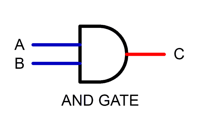
AND Gate Logic Symbol, Boolean Expression & Truth Table
AND Gate Symbol
There are 3 types of symbols used for AND gate all over the world
American National Standards Institute (ANSI)/ MILITARY

International Electrotechnical Commission (IEC)/EUROPEAN

Deutsches Institut für Normung (DIN)/GERMANY

Boolean Expression
C = A.B or C = A & B
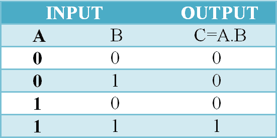
Truth Table
A mathematical table used to specify input to output logic combination of a digital circuit is known as a truth table, the truth table of AND Gate is given below.
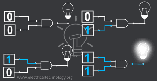
AND Gate Logic Flow Schematic Diagram
Construction and Working Mechanism of AND Gate:
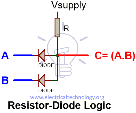
AND Gate using Resistor-Diode Logic(RDL)
In Resistor-Diode Logic (RDL), the diode is used as a switch. In AND Gate, diodes are placed in such configuration when any of the two input is logic-Low “0”, the corresponding diode will become forward bias and logic-Low”0” will flow through output as there is no resistance in its path. When both inputs are logic-High”1” diodes will be reversed biased, Hence Vsupply (Logic High state) will be routed to output C as “1”.
NOTE: There is always diode forward voltage drop of approximately 0.7 volts in the case of silicon and 0.3 volts in the case of the germanium diode.
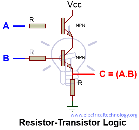
AND Gate using Resistor-Transistor Logic (RTL)
In Resistor-Transistor Logic (RTL), the main switching unit is the transistor. In the figure given below, there are 2 NPN transistors connected in series that switches on with logic level high ”1”, when both of the transistors are turned on, Vcc”1” will flow through output. There is a pull-down resistor connected to the output, Therefore there will be always Logic-Low”0” at the output unless both of the transistors are switched on.
NOTE: RTL logic limitation or disadvantage is that it has high power dissipation due to current flow in base resistors and collector resistors when the BJT’s are switched on.
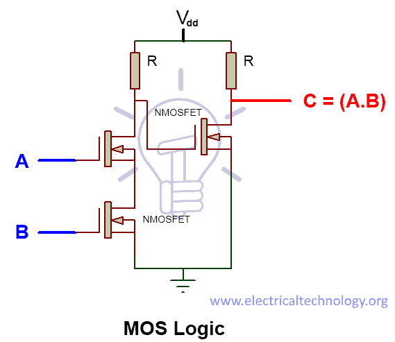
AND Gate using MOS Logic
In MOS Logic, MOSFETs are used as the main switching unit. As you can see in the figure below the two MOSFET in series are being controlled by the inputsignal, In turn, these NMOSFETs control the other NMOSFET. When both inputs are High-State”1”, the NMOS connected in series activates and successively,NMOS on the OUTPUT side is switched off due to logic low gate input (GND). Thus the only route to output is from Vdd (Logic high).
When any of this input is Low-State”0”, the NMOS connected in series will be switched-off resulting in High State”1” at the gate of NMOS on the OUTPUT side(Switched-on). As the NMOS is switched-on, therefore the output C will be directly connected to GND (Low State”0”).
AND Gate From Other Logic Gates
AND gate’s function can be achieved by different combinations of different logic gate some of them are given below.
BOOLEAN EXPRESSION:
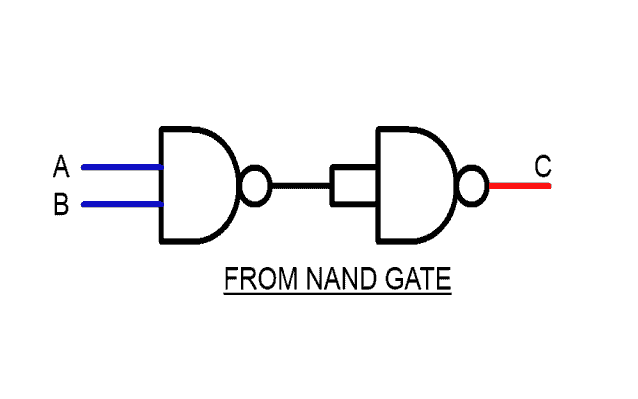
AND Gate From NAND Gate
C = ((A.B)’)’
AND Gate From NOT-NOR Gate
C = A.B
C = (A’+B’)’

AND Gate From NOR GATE
C = (a’+b’)’
C = ((A+A)’ + (B+B)’)’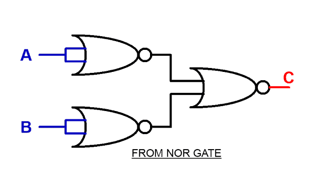
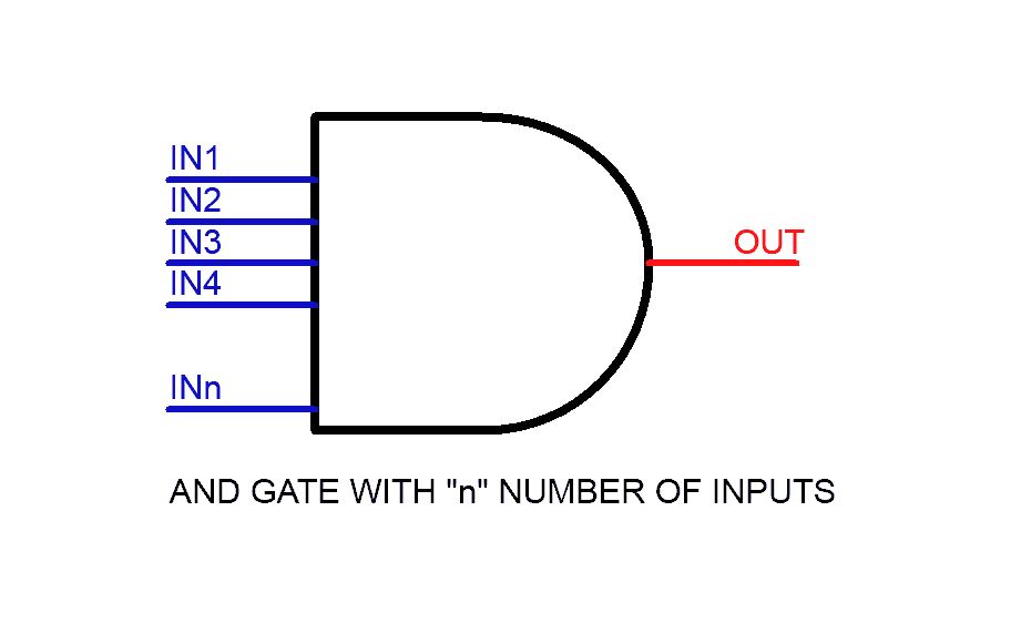
Multiple Input AND Gate
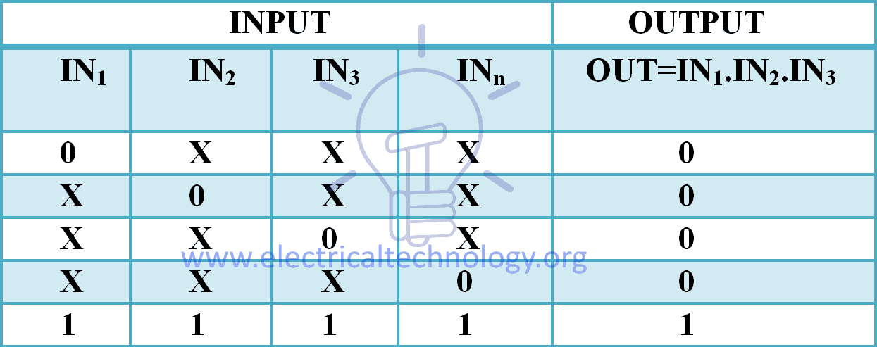
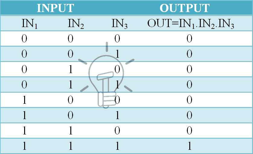
As we have established before that AND Gate gives logic High State”1” only and only when all of its inputs are logic High State”1”. It’s“n” number of inputs truth table is given below:
Truth Table
NOTE: In the table given below “X” means “don’t care”. It can be “1”and it can be “0”. Which means, as long as there is a single input carrying “0”, the output will be always “0” so there is no reason to put a check on other inputs, that’s why it’s called “don’t care X”.
What would you do if there are more than two inputs needed? The answer is simple.
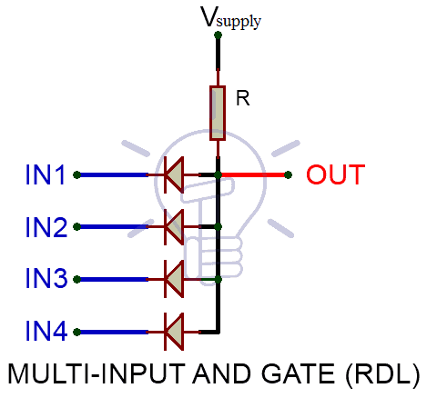
Resistor-Diode Logic
IN RDL (Resistor-Diode logic) logic, a diode is used on every input line, thus adding diodes can increase the number of input lines as shown in the figure below. Each input is fed to separate diode. Place as many diodes as you would like,to create a Multi-Input AND GATE.
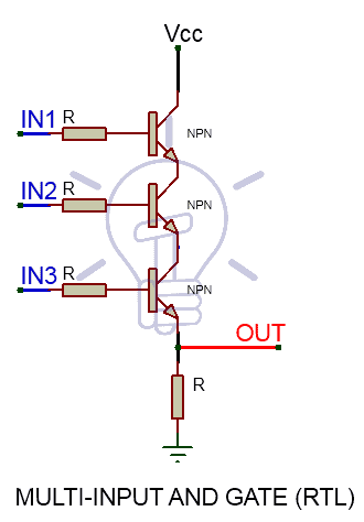
 Resistor-Transistor Logic
In RTL (Resistor-Transistor Logic), Transistors are used as switching unit. To increase the input lines we have to increase the number of transistors connected in series as shown in the figure below.
MOS Logic
In MOS logic, the case is same as RTL logic, instead, we increase the number of MOSFETs connected in series at the input side. AND GATE with three input in MOS logic is given below. If you want to add another input, add another NMOS in series.
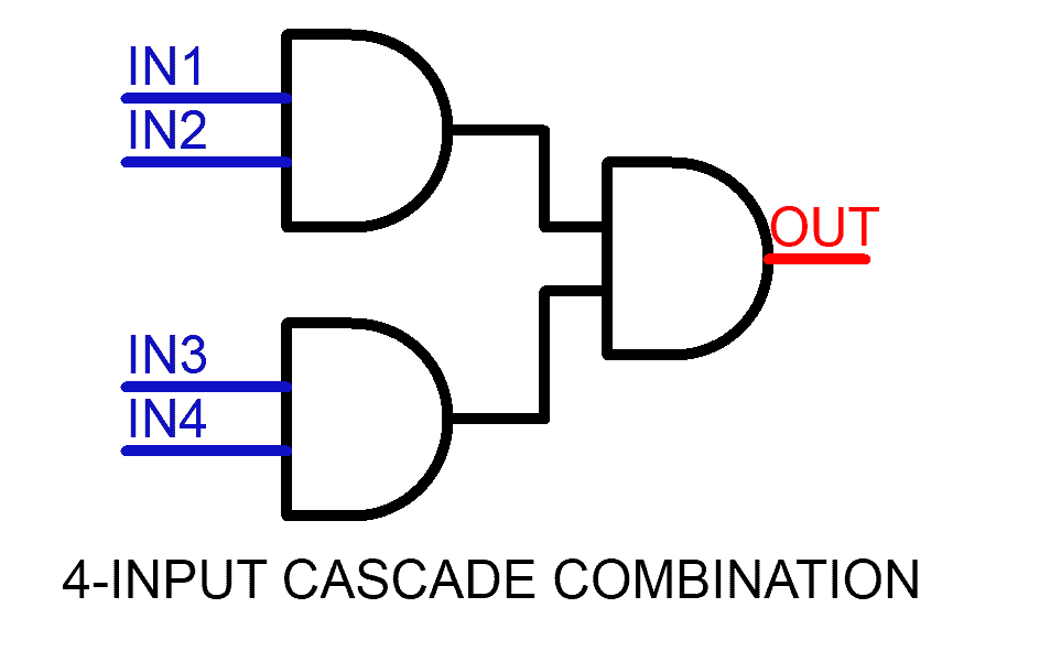
Cascaded Setup of AND Gates
Multi-input AND gate function can be achieved by cascading Two-Input AND Gate in a specific configuration given below
OUT = IN1 & IN2 & IN3
OUT = (IN1 & IN2) & IN3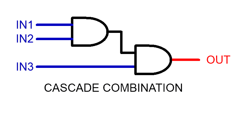
OUT = IN1 & IN2 & IN3 & IN4
OUT = (IN1 & IN2) & (IN3 & IN4)
TTL and CMOS Logic AND Gate IC’s
Commercially up to Four-Input AND gate IC’s are available in the market, having two AND gates in a single package. Some of the ICs with Pin Details are given below.
TTL Logic AND Gates
- 74LS08 Quad 2-input
- 74LS11 Triple 3-input
- 74LS21 Dual 4-input
CMOS Logic AND Gates
- CD4081 Quad 2-input
- CD4073 Triple 3-input
- CD4082 Dual 4-input
7408 TTL and 4081 CMOS AND Gate IC (Two-Inputs)
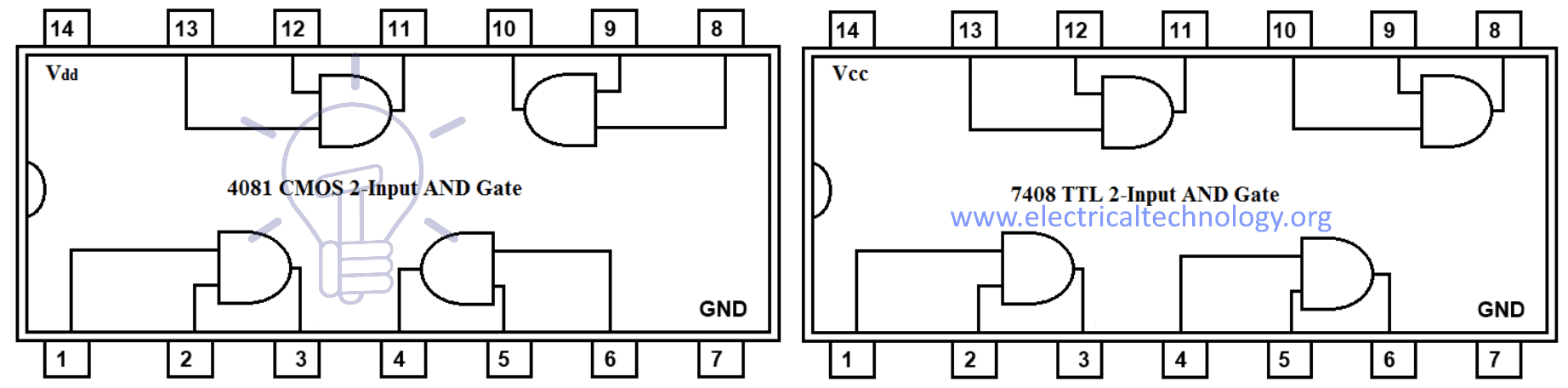
Pinout for 7408 TTL AND Gate IC
| PIN Number | Description |
| 1 | Input Gate 1 |
| 2 | Input Gate 1 |
| 3 | Output Gate 1 |
| 4 | Input Gate 2 |
| 5 | Input Gate 2 |
| 6 | Output Gate 2 |
| 7 | Ground |
| 8 | Output Gate 3 |
| 9 | Input Gate 3 |
| 10 | Input Gate 3 |
| 11 | Output Gate 4 |
| 12 | Input Gate 4 |
| 13 | Input Gate 4 |
| 14 | Positive Supply Voltage |
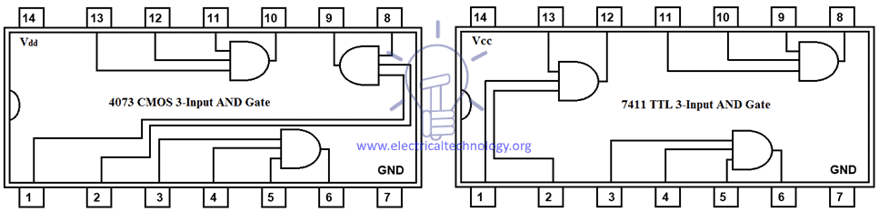
4073 CMOS and 7411 TTL AND Gate IC (Three-Inputs)
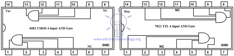
4082 CMOS and 7821 TTL AND Gate IC (Four-Inputs)
AND Gate Applications
Common uses and application of AND gate are follow:
- As enable gate (Allowance of data through a channel).
- As inhibit gate (Reverse of enable gate i.e. disallowance of data through a channel).
- In the clock counters as enable and disable gate.
- Used in security devices e.g security lights and flood lights as PIR (Passive infrared) Device.
- In most of counting, computers and logic based digital circuits,
You may also read:
Digital Logic OR Gate Digital Logic NOT GateThe post Digital Logic AND Gate appeared first on Electrical Technology.
April 14, 2018 at 02:43AM by Department of EEE, ADBU: https://ift.tt/2AyIRVT