Digital Flip-Flops – Types & Operation of Flip-Flops
What is Flip-Flop?
Digital flip-flops are memory devices used for storing binary data in sequential logic circuits. Latches are level sensitive and Flip-flops are edge sensitive. It means that the latch’s output change with a change in input levels and the flip-flop’s output only change when there is an edge of controlling signal. That control signal is known as a clock signal Q.
Types of Digital Flip-Flops
Most common types of flip-flops are as follow.
- SR Flip-flop
- D Flip-flop
- JK Flip-flop
- T Flip-flop
- You may also read: Ripple Carry And Carry Look Ahead Adder
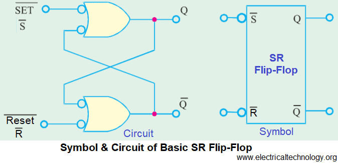
SR Flip-Flop
SR Flip-flop is the most basic sequential logic circuit also known as SR latch. It has two inputs known as SET and RESET. The Output “Q” is High if the input as SET is High (when the clock is triggered). If the input RESET is High when the clock is triggered, the Output “Q” would be “LOW”. Note that both the Inputs i.e. SET and RESET should not be “High” when the clock is triggered as it is considers as invalid input condition which leads to unpredictable output result.
Symbol and Circuit of Basic SR Flip-Flop
Truth Table of SR Flip-Flop
Below is the Truth table of SET-RESET Function of SR Flip-Flop.
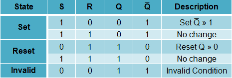 It is clear from the truth table that
If
S =1 , R = 1, then Q and Q̅ may be logic level 1 or 0.
S =0 , R = 0, = it is invalid condition and must be avoided. The rest can be seen in the above truth table.
D Flip-Flop
D Flip-flop operation is same as D latch. The only difference is that D flip-flop changes its output only when there is an edge of the clock signal.
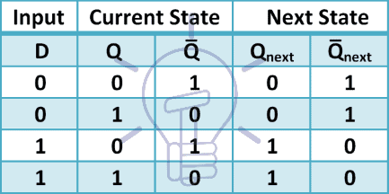
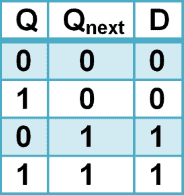
Truth Table
Flip-flop’s truth table consists of current and next states. It shows the output state of flip-flop after a clock cycle.
The truth table for D flip-flop is given below:
Characteristic Table
A characteristic table is a short form of the truth table. It provides the information about what the next state of the flip-flop will be on a specific input. The characteristic table of D flip-flop is given below.
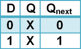
X means don’t care. It does not matter what the current state is for this input, the next state is guaranteed.
Excitation Table
Excitation table shows the necessary inputs for a current state to change into a specific next state. Excitation table of D flip-flop is given below:
Construction of D Flip-Flop
D flip-flop is made from 2 D-latches. Its schematic is given in the figure below:
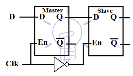
The first latch is master D-latch and the second one is slave-latch. When clk = 1 the master latch will be enabled and slave latch will be disabled. The master latch will evaluate its output state as Qm = D but it will not be processed by slave latch. When clk becomes 0, the master latch will get disabled and it will not change its state and the slave latch will get enabled. The output of slave latch will get updated as Q = Qm = D. it shows that the output state only changes when the clock signal goes from 1 to 0, meaning negative or falling edge of the clock signal.
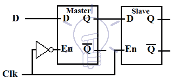
We can also design it for positive or rising edge. To change it to rising edge sensitive, we have to attach inverter with master latch’s enable pin as shown in the figure given below:
D Flip-flop can also be made using 3 S-R latches using 6 NAND gates. It is efficient as it uses less logic gate for fast speed and low cost. Its schematic is given below:
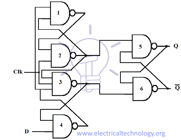
When clk = 0 , then S = 1 and R = 1, which is hold state for NAND gate SR latch. The flip-flop will hold its state.
When clk = 1 and D =1 then gate 4 output = 0 because R = 1. One input of gate 3 is low “0”, so its output = 1, which is R = 1. One input of gate 1 is low so its output = 1. That makes the output of gate 2 S = 0 because both inputs are high. R = 1, S = 0 will set the output state Q = 1.
Now if clk = 0 the S,R = 1 & the flip-flop will hold the current state.
Again when clk = 1 and D = 0. Both inputs to the gate 4 are high, so the output of gate 4 R = 0.it will reset the output state Q = 0.
Thus this flip-flop works on positive or rising edge of the clock signal.
S,R state does not go to hold state until the clock signal = 0.
D Flip-Flop with Enable
Enable pin enables the D flip-flop to hold its last state without considering the clock signal. It does not matter if there is a clock edge, the flip-flop will hold its state if it is disabled. Its schematic is given below.
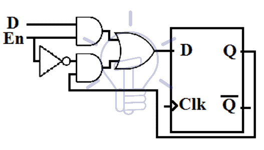
When En = 0, the flip-flop will retains its state & when En = 1, it can change its state upon next clock cycle.
JK Flip-Flop
JK flip-flop is same as S-R flip-flop but without any restricted input. The restricted input of S-R latch toggles the output of JK flip-flop.
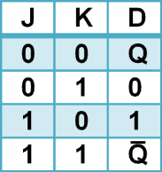
JK flip-flop is modified version of D flip-flop. We attach a combinational circuit to a D flip-flop to convert it into JK flip-flop. Its state table is given below:
Characteristic Table
A characteristic table is ashort form of the truth table. It provides the information about what the next state of the flip-flop will be on a specific input. The characteristic table of JK flip-flop is given below.
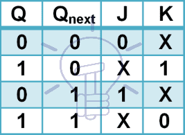
Excitation Table
Excitation table shows the necessary inputs for a current state to change into a specific next state. Excitation table of JK flip-flop is given below:
Truth Table
The truth table of JK flip-flop is given below:
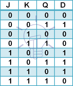
Solving the truth table using K-map, the expression for D is:
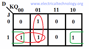
D = K̅Q + JQ̅
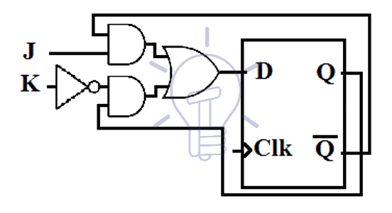
Its schematic is given in the figure below.
Symbol
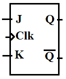
The symbol for positive or rising edge sensitive JK flip-flop is given below:
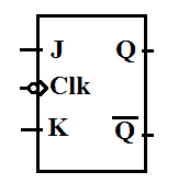
The symbol for negative or falling edge sensitive JK flip-flop is given below.
JK flip-flop eliminates the problem of restricted input of SR flip-flop.
T Flip-Flop
T stands for the toggle. T flip-flop is modified version of JK flip-flop. JK inputs of JK flip-flop combine together to form a single input T. This flip-flop is called T flip-flop.
When T = 1, the output keeps changing Q = Q̅ upon each clock cycle.
When T = 0, the flip-flop hold its state Q = Q.
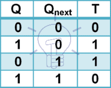
Characteristic Table
The characteristic table shows the short form of the truth table. T flip-flop characteristic table is given below:

Excitation Table
Its excitation table is given below:
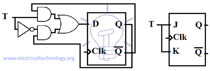
The schematic of T flip-flop is given below:
Symbol
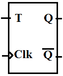
The symbol for positive or rising edge sensitive T flip-flop is given below:
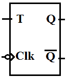
The symbol for negative or falling edge sensitive T flip-flop is given below.
Application of Digital Flip-Flops
Following are the common application of
- Data storage and transfer
- Flip-Flop synchronization
- Serial data transfer-shift register
- Frequency division
- Counting
- Event detectors
You may also read more about Digital Logic gates
Digital Logic NOT Gate – Digital Inverter Logic Gate
Digital Logic OR Gate
Digital Logic AND Gate
Exclusive-NOR (XNOR) Digital Logic Gate
Digital Logic NOR Gate
Digital Logic NAND Gate
The post Digital Flip-Flops – SR, D, JK and T Flip Flops appeared first on Electrical Technology.
May 01, 2018 at 10:33PM by Department of EEE, ADBU: https://ift.tt/2AyIRVT