Explore USB power solutions that handle more power, enable smarter charging, and simplify designs. Find out more! Renesas Electronics Corporation has introduced two new integrated circuits (ICs): the RAA489118 buck-boost battery charger and the RAA489400 USB Type-C port controller. These ICs provide an Extended Power Range (EPR) USB Power Delivery (PD) solution. The company claims […]
View more at https://www.electronicsforu.com/news/usb-power-solutions-for-extended-power-range.
Credit- EFY. Distributed by Department of EEE, ADBU: https://tinyurl.com/eee-adbu
Curated by Jesif Ahmed
Maintenance Practices to be Followed for On-Site Generator Overhauling

This discussion will focus on the on-site overhauling of a gas-powered generator, detailing the essential procedures for its enhancement. It is a common practice for utilities to test electrical assets periodically after a certain interval of time mainly as part... Read more
The post Maintenance Practices to be Followed for On-Site Generator Overhauling appeared first on EEP - Electrical Engineering Portal.
View more at: https://electrical-engineering-portal.com/maintenance-practices-on-site-generator-overhauling Credit- EEE - Electrical Engineering Portal. Distributed by Department of EEE, ADBU: https://tinyurl.com/eee-adbu
Curated by Jesif Ahmed.
Smarter Eye-Tracking For Smart Glasses
The ETH Zurich team introduces ElectraSight, a hybrid eye-tracking system for smart glasses, combining contact and contactless methods. Smart glasses are getting smarter and offering new ways to interact with devices and the world around us. Eye movements are one of the simplest and most natural ways to use them. By tracking where we look, […]
View more at https://www.electronicsforu.com/news/smarter-eye-tracking-for-smart-glasses.
Credit- EFY. Distributed by Department of EEE, ADBU: https://tinyurl.com/eee-adbu
Curated by Jesif Ahmed
View more at https://www.electronicsforu.com/news/smarter-eye-tracking-for-smart-glasses.
Credit- EFY. Distributed by Department of EEE, ADBU: https://tinyurl.com/eee-adbu
Curated by Jesif Ahmed
Real-Time CO2 Status Indicator and Monitor with BleuIO and Renesas EK-RA4M2
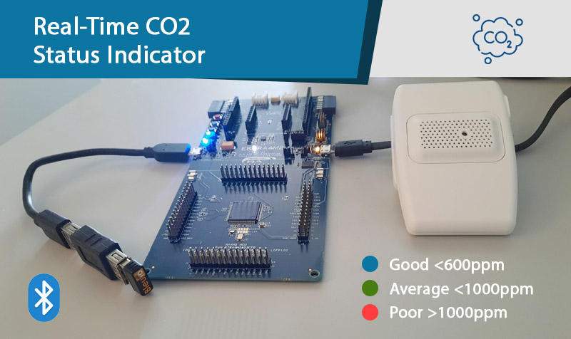
Introduction In an age where air quality has become increasingly important, monitoring CO2 levels in various...
The post Real-Time CO2 Status Indicator and Monitor with BleuIO and Renesas EK-RA4M2 appeared first on Electronics-Lab.com.
View more at https://www.electronics-lab.com/real-time-co2-status-indicator-and-monitor-with-bleuio-and-renesas-ek-ra4m2/.
Credit- ELECTRONICS-LAB. Distributed by Department of EEE, ADBU: https://tinyurl.com/eee-adbu
Curated by Jesif Ahmed
Lithium-Ion Battery Tech Enhances Cathode Durability
This research offers a promising path forward for next-generation cathode development, paving the way for more durable and efficient lithium-ion batteries critical to electric vehicles and energy storage systems. A research team at Pohang University of Science and Technology has unveiled strategy to significantly improve the durability of lithium-rich layered oxide (LLO) materials, a next-generation […]
View more at https://www.electronicsforu.com/news/lithium-ion-battery-tech-enhances-cathode-durability.
Credit- EFY. Distributed by Department of EEE, ADBU: https://tinyurl.com/eee-adbu
Curated by Jesif Ahmed
View more at https://www.electronicsforu.com/news/lithium-ion-battery-tech-enhances-cathode-durability.
Credit- EFY. Distributed by Department of EEE, ADBU: https://tinyurl.com/eee-adbu
Curated by Jesif Ahmed
IoT Module With Wi-Fi 6 And Bluetooth 5.3 Enhances Connectivity
A latest wireless IoT module simplifies edge connectivity, integrating STM32 and Qualcomm technologies. STMicroelectronics, a global leader in semiconductor solutions, has launched its first wireless IoT module developed in collaboration with Qualcomm Technologies. Designed to enhance consumer and industrial IoT development, the ST67W611M1 module leverages the STM32 ecosystem and Qualcomm’s wireless connectivity expertise. The new […]
View more at https://www.electronicsforu.com/news/iot-module-with-wi-fi-6-and-bluetooth-5-3-enhances-connectivity.
Credit- EFY. Distributed by Department of EEE, ADBU: https://tinyurl.com/eee-adbu
Curated by Jesif Ahmed
View more at https://www.electronicsforu.com/news/iot-module-with-wi-fi-6-and-bluetooth-5-3-enhances-connectivity.
Credit- EFY. Distributed by Department of EEE, ADBU: https://tinyurl.com/eee-adbu
Curated by Jesif Ahmed
Real-Time Visualization Of Stretchable Electronics
What if you could see how stretchable electronics deform in real time without relying on simulations or damage? Learn more! A research team at POSTECH has developed a new technology to analyze and visualize, in real-time, the deformation of “serpentine” structures—key components in stretchable electronics. The process is displayed through colour changes. Stretchable electronics have […]
View more at https://www.electronicsforu.com/news/real-time-visualization-of-stretchable-electronics.
Credit- EFY. Distributed by Department of EEE, ADBU: https://tinyurl.com/eee-adbu
Curated by Jesif Ahmed
View more at https://www.electronicsforu.com/news/real-time-visualization-of-stretchable-electronics.
Credit- EFY. Distributed by Department of EEE, ADBU: https://tinyurl.com/eee-adbu
Curated by Jesif Ahmed
Autoranging True RMS Multimeter
This instrument ensures precise results in even the most challenging environments, featuring a 60,000-count display, 21 functions, 63 ranges, and robust features like data logging, temperature measurement, and IP65 protection. KUSAM-MECO has introduced the advanced TRMS Digital Multimeter Model KM 891 instrument designed to provide high accuracy, versatility, and durability for professional use. With 60,000 […]
View more at https://www.electronicsforu.com/news/autoranging-true-rms-multimeter.
Credit- EFY. Distributed by Department of EEE, ADBU: https://tinyurl.com/eee-adbu
Curated by Jesif Ahmed
View more at https://www.electronicsforu.com/news/autoranging-true-rms-multimeter.
Credit- EFY. Distributed by Department of EEE, ADBU: https://tinyurl.com/eee-adbu
Curated by Jesif Ahmed
SSD With A Lifespan Of Up To 1200TBW
The new SK Hynix SSD based on non-volatile memory express technology, promises lightning-fast performance and efficiency for Indian consumers. A novel solid-state drive (SSD) developed by SK Hynix, the Platinum P41, has been introduced to the Indian market by Irvine, a prominent distributor of memory products. This advanced storage solution is poised to meet the […]
View more at https://www.electronicsforu.com/news/ssd-with-a-lifespan-of-up-to-1200tbw.
Credit- EFY. Distributed by Department of EEE, ADBU: https://tinyurl.com/eee-adbu
Curated by Jesif Ahmed
View more at https://www.electronicsforu.com/news/ssd-with-a-lifespan-of-up-to-1200tbw.
Credit- EFY. Distributed by Department of EEE, ADBU: https://tinyurl.com/eee-adbu
Curated by Jesif Ahmed
Sodium-Ion Batteries With 458Wh/kg Energy Density
Researchers discovered a novel material to improve sodium-ion batteries, offering a sustainable and cost-effective alternative to lithium-based technologies. A new material developed by an international team of scientists, including researchers from the University of Houston, has set a milestone in energy storage technology. The material, sodium vanadium phosphate (NaxV2(PO4)3), significantly enhances the performance of sodium-ion […]
View more at https://www.electronicsforu.com/news/sodium-ion-batteries-with-458wh-kg-energy-density.
Credit- EFY. Distributed by Department of EEE, ADBU: https://tinyurl.com/eee-adbu
Curated by Jesif Ahmed
View more at https://www.electronicsforu.com/news/sodium-ion-batteries-with-458wh-kg-energy-density.
Credit- EFY. Distributed by Department of EEE, ADBU: https://tinyurl.com/eee-adbu
Curated by Jesif Ahmed
Lanner NCA-1050: Fanless Gateway with Intel Atom X7835RE/X7405C/X7203C for Secure Edge and AI Workloads
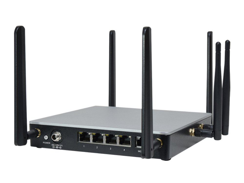
The Lanner NCA-1050 is a fanless gateway appliance designed for small and medium-sized businesses (SMBs), offering...
The post Lanner NCA-1050: Fanless Gateway with Intel Atom X7835RE/X7405C/X7203C for Secure Edge and AI Workloads appeared first on Electronics-Lab.com.
View more at https://www.electronics-lab.com/lanner-nca-1050-fanless-gateway-with-intel-atom-x7835re-x7405c-x7203c-for-secure-edge-and-ai-workloads/.
Credit- ELECTRONICS-LAB. Distributed by Department of EEE, ADBU: https://tinyurl.com/eee-adbu
Curated by Jesif Ahmed
AMPCOM 9-Port 2.5GbE Switch with Web Management, 10G SFP+ uplink, and QoS for Office and Surveillance Networks

The AMPCOM 2.5GbE Managed Switch is a high-performance 9-port Ethernet switch featuring 8 RJ45 ports (100/1000/2500...
The post AMPCOM 9-Port 2.5GbE Switch with Web Management, 10G SFP+ uplink, and QoS for Office and Surveillance Networks appeared first on Electronics-Lab.com.
View more at https://www.electronics-lab.com/ampcom-9-port-2-5gbe-switch-with-web-management-10g-sfp-uplink-and-qos-for-office-and-surveillance-networks/.
Credit- ELECTRONICS-LAB. Distributed by Department of EEE, ADBU: https://tinyurl.com/eee-adbu
Curated by Jesif Ahmed
Flyback Transformer Provides 10mm Creepage For High Isolation
A flyback transformer launched to enhance isolation, safety, and efficiency in compact designs for electric vehicles and energy storage systems. An innovative flyback transformer designed to improve power density and safety in automotive and industrial applications has been launched by Bourns, California. This innovation, the ‘HVMA03F40C-ST10S flyback transformer’, aligns with AEC-Q200 automotive-grade compliance, delivering enhanced performance […]
View more at https://www.electronicsforu.com/news/flyback-transformer-provides-10mm-creepage-for-high-isolation.
Credit- EFY. Distributed by Department of EEE, ADBU: https://tinyurl.com/eee-adbu
Curated by Jesif Ahmed
View more at https://www.electronicsforu.com/news/flyback-transformer-provides-10mm-creepage-for-high-isolation.
Credit- EFY. Distributed by Department of EEE, ADBU: https://tinyurl.com/eee-adbu
Curated by Jesif Ahmed
Gas Discharge Tube With Voltage Support Up To 600V
A new ultra-compact gas discharge tube series ensures reliable surge protection for industrial and communication systems, engineered for space-constrained applications. Bourns, California, has introduced the model GDT21 Gas Discharge Tube (GDT) series, the latest surge protection device tailored for compact industrial and communication setups. This 2-electrode GDT offers enhanced transient voltage protection to shield systems […]
View more at https://www.electronicsforu.com/news/gas-discharge-tube-with-voltage-support-up-to-600v.
Credit- EFY. Distributed by Department of EEE, ADBU: https://tinyurl.com/eee-adbu
Curated by Jesif Ahmed
View more at https://www.electronicsforu.com/news/gas-discharge-tube-with-voltage-support-up-to-600v.
Credit- EFY. Distributed by Department of EEE, ADBU: https://tinyurl.com/eee-adbu
Curated by Jesif Ahmed
Chip Design Improves Performance Without Silicon
An electronic stacking method could significantly increase the number of chip transistors, improving AI hardware efficiency. MIT engineers have created a new type of chip that doesn’t need silicon wafers and works at lower temperatures to protect the circuits underneath. This method lets them build chips with materials stacked directly on each other, allowing components […]
View more at https://www.electronicsforu.com/news/chip-design-improves-performance-without-silicon.
Credit- EFY. Distributed by Department of EEE, ADBU: https://tinyurl.com/eee-adbu
Curated by Jesif Ahmed
View more at https://www.electronicsforu.com/news/chip-design-improves-performance-without-silicon.
Credit- EFY. Distributed by Department of EEE, ADBU: https://tinyurl.com/eee-adbu
Curated by Jesif Ahmed
AAEON’s New uCOM-IMX8P Brings RISC Computing to its SMARC Module Portfolio
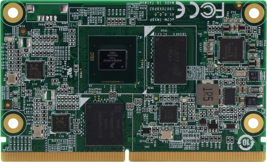
AAEON’s expansion into new architectures proves to be worth the RISC. AAEON, a leader in industrial...
The post AAEON’s New uCOM-IMX8P Brings RISC Computing to its SMARC Module Portfolio appeared first on Electronics-Lab.com.
View more at https://www.electronics-lab.com/aaeons-new-ucom-imx8p-brings-risc-computing-to-its-smarc-module-portfolio/.
Credit- ELECTRONICS-LAB. Distributed by Department of EEE, ADBU: https://tinyurl.com/eee-adbu
Curated by Jesif Ahmed
LIVE DIY: Energy-Saving Light With Built-In Security Alert
In this session, you’ll learn to build your own home security and power-saving light—perfect for keeping your home safe and reducing your electricity bills! What You’ll Learn
View more at https://www.electronicsforu.com/videos-slideshows/live-diy-energy-saving-light-with-builtin-security-alert.
Credit- EFY. Distributed by Department of EEE, ADBU: https://tinyurl.com/eee-adbu
Curated by Jesif Ahmed
View more at https://www.electronicsforu.com/videos-slideshows/live-diy-energy-saving-light-with-builtin-security-alert.
Credit- EFY. Distributed by Department of EEE, ADBU: https://tinyurl.com/eee-adbu
Curated by Jesif Ahmed
Strain-Enhanced Potassium Niobate Withstands 701°C
Researchers developed a novel technique called “atomic spray painting” to enhance potassium niobate’s properties for greener and more efficient technologies. In the latest research scientists from Penn State Department of Materials Science and Engineering used molecular beam epitaxy (MBE) to strain-tune potassium niobate—a key material in advanced electronics. By adjusting the material’s atomic structure, they […]
View more at https://www.electronicsforu.com/news/strain-enhanced-potassium-niobate-withstands-701c.
Credit- EFY. Distributed by Department of EEE, ADBU: https://tinyurl.com/eee-adbu
Curated by Jesif Ahmed
View more at https://www.electronicsforu.com/news/strain-enhanced-potassium-niobate-withstands-701c.
Credit- EFY. Distributed by Department of EEE, ADBU: https://tinyurl.com/eee-adbu
Curated by Jesif Ahmed
Affordable Infrared Lasers For Photonics Technology
A novel laser innovation using lead sulphide quantum dots offers cost-effective, scalable, and silicon-compatible solutions for extended SWIR applications. A team of researchers at ICFO—The Institute of Photonic Sciences, has developed a novel laser technology using lead sulphide colloidal quantum dots (CQDs). This advancement enables coherent light emission in the extended short-wave infrared (SWIR) spectrum, […]
View more at https://www.electronicsforu.com/news/affordable-infrared-lasers-for-photonics-technology.
Credit- EFY. Distributed by Department of EEE, ADBU: https://tinyurl.com/eee-adbu
Curated by Jesif Ahmed
View more at https://www.electronicsforu.com/news/affordable-infrared-lasers-for-photonics-technology.
Credit- EFY. Distributed by Department of EEE, ADBU: https://tinyurl.com/eee-adbu
Curated by Jesif Ahmed
MYIR Introduces the MYC-LT536 System-On-Module
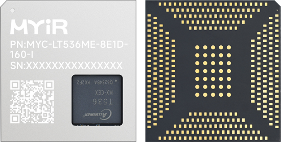
Measuring only 43mm by 45mm, the MYC-LT536 is a compact System-On-Module (SOM) based on the Allwinner...
The post MYIR Introduces the MYC-LT536 System-On-Module appeared first on Electronics-Lab.com.
View more at https://www.electronics-lab.com/myir-introduces-the-myc-lt536-system-on-module/.
Credit- ELECTRONICS-LAB. Distributed by Department of EEE, ADBU: https://tinyurl.com/eee-adbu
Curated by Jesif Ahmed
Signaloid C0-microSD Is A Compact Programmable FPGA SoM in MicroSD Form Factor
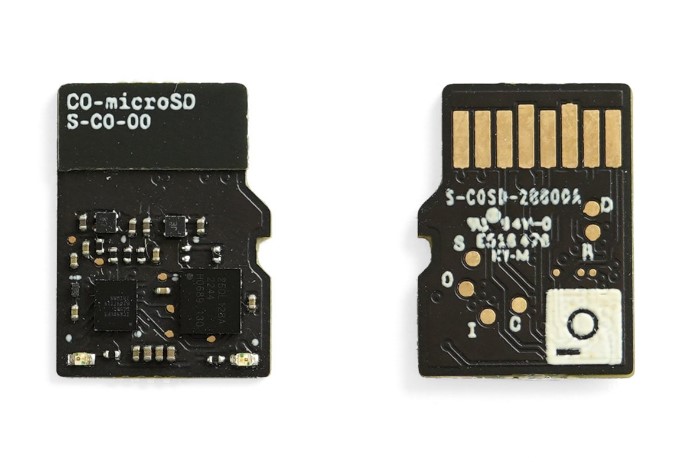
The Signaloid C0-microSD is built around Lattice Semiconductor’s iCE40UPK FPGA, designed to provide versatile computing options...
The post Signaloid C0-microSD Is A Compact Programmable FPGA SoM in MicroSD Form Factor appeared first on Electronics-Lab.com.
View more at https://www.electronics-lab.com/signaloid-c0-microsd-is-a-compact-programmable-fpga-som-in-microsd-form-factor/.
Credit- ELECTRONICS-LAB. Distributed by Department of EEE, ADBU: https://tinyurl.com/eee-adbu
Curated by Jesif Ahmed
Compact 600 V Solid-State Relay
Compact, Industrial-Grade Device Features 0.3 ms Typical Fast Turn-On Time and Ultra-Low Leakage Current of 2 nA. Vishay Intertechnology, Inc. has unveiled the VOR1060M4, a 1 Form A solid-state relay designed for advanced energy storage, industrial, and mobility applications. This new product delivers a 600 V load voltage and 3750 VRMS isolation voltage within a […]
View more at https://www.electronicsforu.com/news/compact-600-v-solid-state-relay.
Credit- EFY. Distributed by Department of EEE, ADBU: https://tinyurl.com/eee-adbu
Curated by Jesif Ahmed
View more at https://www.electronicsforu.com/news/compact-600-v-solid-state-relay.
Credit- EFY. Distributed by Department of EEE, ADBU: https://tinyurl.com/eee-adbu
Curated by Jesif Ahmed
5000m High Altitude Ready DC/DC Converters
Compact converters for power solutions addressing diverse applications with advanced protection, rugged performance, and space-saving designs. A new series of compact DC/DC converters, TEC 3UI, has been developed by Traco Powers, offering an ultra-wide 8:1 input range. Designed for industrial operations, these converters ensure versatility and reliability across varying conditions, making them an attractive choice […]
View more at https://www.electronicsforu.com/news/5000m-high-altitude-ready-dc-dc-converters.
Credit- EFY. Distributed by Department of EEE, ADBU: https://tinyurl.com/eee-adbu
Curated by Jesif Ahmed
View more at https://www.electronicsforu.com/news/5000m-high-altitude-ready-dc-dc-converters.
Credit- EFY. Distributed by Department of EEE, ADBU: https://tinyurl.com/eee-adbu
Curated by Jesif Ahmed
Fixed-Direction Voltage Level Translators
The voltage translation solution reduces power use and improves performance, simplifying communication across various applications. Find out more. Nexperia has launched a new family of fixed-direction voltage level translators designed for use with push-pull data interfaces such as UART, SPI, and JTAG, as well as general-purpose input/output (GPIO). The NXU series includes 4-bit, 2-bit, and […]
View more at https://www.electronicsforu.com/news/fixed-direction-voltage-level-translators.
Credit- EFY. Distributed by Department of EEE, ADBU: https://tinyurl.com/eee-adbu
Curated by Jesif Ahmed
View more at https://www.electronicsforu.com/news/fixed-direction-voltage-level-translators.
Credit- EFY. Distributed by Department of EEE, ADBU: https://tinyurl.com/eee-adbu
Curated by Jesif Ahmed
Power Supplies With Tool-Free Push-In Wire Terminations
Designed for automation, the design eliminates the need for tools, reducing assembly time and costs while ensuring long-term operational excellence. TDK Corporation has unveiled push-in wire termination options for its high-reliability TDK-Lambda HWS-A family of AC-DC power supplies. The new HWS-A/E models, available with vertical or horizontal terminal orientations, simplify cable harnessing and are designed […]
View more at https://www.electronicsforu.com/news/power-supplies-with-tool-free-push-in-wire-terminations.
Credit- EFY. Distributed by Department of EEE, ADBU: https://tinyurl.com/eee-adbu
Curated by Jesif Ahmed
View more at https://www.electronicsforu.com/news/power-supplies-with-tool-free-push-in-wire-terminations.
Credit- EFY. Distributed by Department of EEE, ADBU: https://tinyurl.com/eee-adbu
Curated by Jesif Ahmed
Light Emitting Fibre With Luminance of 1068 cd/m²
Researchers at NUS have developed SHINE fibres, offering self-healing, light-emitting, and magnetic properties for advancements in robotics, wearable technology, and smart textiles. A unique light-emitting fibre with self-healing and magnetic properties has been developed at the National University of Singapore (NUS). The scalable hydrogel-clad ionotronic nickel-core electroluminescent fibre (SHINE), offers a unique blend of flexibility, […]
View more at https://www.electronicsforu.com/news/light-emitting-fibre-with-luminance-of-1068-cd-m%c2%b2.
Credit- EFY. Distributed by Department of EEE, ADBU: https://tinyurl.com/eee-adbu
Curated by Jesif Ahmed
View more at https://www.electronicsforu.com/news/light-emitting-fibre-with-luminance-of-1068-cd-m%c2%b2.
Credit- EFY. Distributed by Department of EEE, ADBU: https://tinyurl.com/eee-adbu
Curated by Jesif Ahmed
Measures to reduce interference from Variable Speed Drives

Often referred to as Variable Frequency Drives, AC Variable Speed Drives (VSD) generate a great deal of electrical interference. Pulse Width Modulation (PWM) is the standard method for controlling motor speed in VSDs. The quick rise and fall times of... Read more
The post Measures to reduce interference from Variable Speed Drives appeared first on EEP - Electrical Engineering Portal.
View more at: https://electrical-engineering-portal.com/measures-to-reduce-interference-from-variable-speed-drives Credit- EEE - Electrical Engineering Portal. Distributed by Department of EEE, ADBU: https://tinyurl.com/eee-adbu
Curated by Jesif Ahmed.
AAEON Releases its First Meteor Lake-Powered Mini AI PC with the UP Xtreme i14 Edge
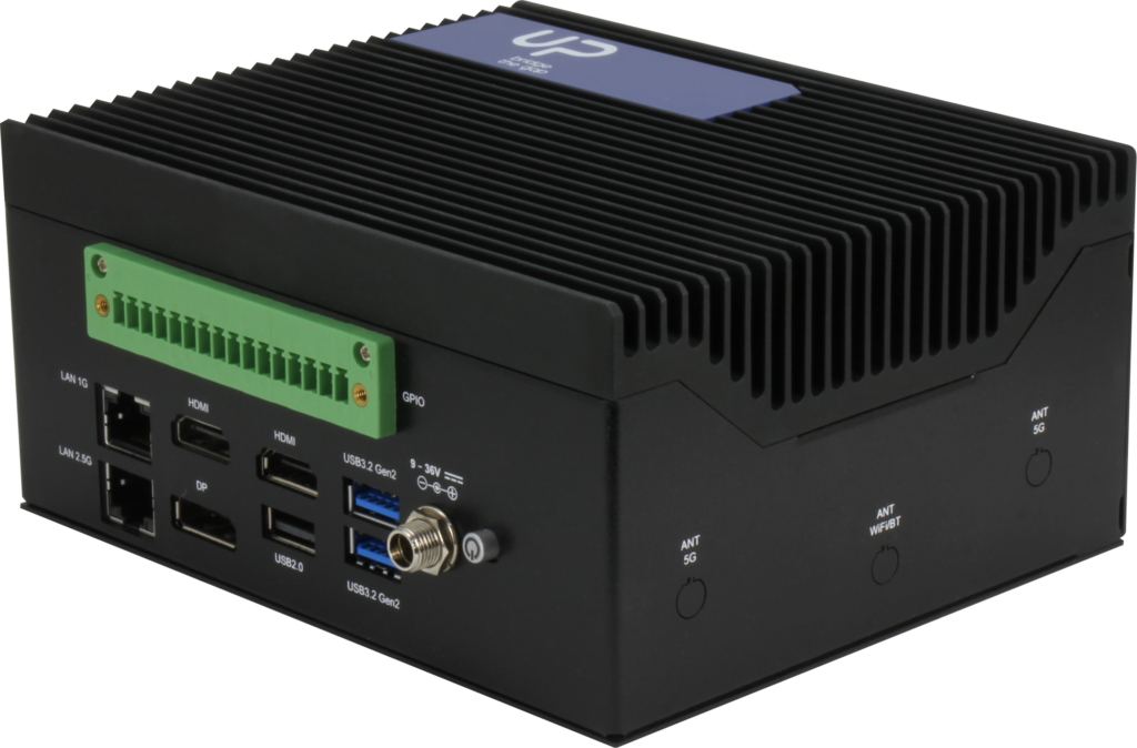
Double the system memory, a substantial graphics boost, and more advanced display interfaces combine to create...
The post AAEON Releases its First Meteor Lake-Powered Mini AI PC with the UP Xtreme i14 Edge appeared first on Electronics-Lab.com.
View more at https://www.electronics-lab.com/aaeon-releases-its-first-meteor-lake-powered-mini-ai-pc-with-the-up-xtreme-i14-edge/.
Credit- ELECTRONICS-LAB. Distributed by Department of EEE, ADBU: https://tinyurl.com/eee-adbu
Curated by Jesif Ahmed
Emergency Lighting Addressing Train Safety Measures
An advanced emergency light unit (ELU) promises uninterrupted lighting in train coaches during emergencies. A new emergency light unit (ELU), developed to enhance passenger safety during power outages and emergencies, has been introduced for Indian railways. Designed by MIC electronics limited (MICEL), a leader in LED lighting and display technologies, the ELU is poised for […]
View more at https://www.electronicsforu.com/news/emergency-lighting-addressing-train-safety-measures.
Credit- EFY. Distributed by Department of EEE, ADBU: https://tinyurl.com/eee-adbu
Curated by Jesif Ahmed
View more at https://www.electronicsforu.com/news/emergency-lighting-addressing-train-safety-measures.
Credit- EFY. Distributed by Department of EEE, ADBU: https://tinyurl.com/eee-adbu
Curated by Jesif Ahmed
Renesas RX260 and RX261 Microcontrollers Deliver High Efficiency and Advanced Touch Features with Security Functions

Renesas has recently introduced the RX260 and RX261, 32-bit microcontrollers designed for outstanding power efficiency, advanced...
The post Renesas RX260 and RX261 Microcontrollers Deliver High Efficiency and Advanced Touch Features with Security Functions appeared first on Electronics-Lab.com.
View more at https://www.electronics-lab.com/renesas-rx260-and-rx261-microcontrollers-deliver-high-efficiency-and-advanced-touch-features-with-security-functions/.
Credit- ELECTRONICS-LAB. Distributed by Department of EEE, ADBU: https://tinyurl.com/eee-adbu
Curated by Jesif Ahmed
Microchip PIC64HX1000 64-bit AI MPU delivers Post-Quantum Security for aerospace, defense, and automotive applications

Microchip recently released the PIC64HX1000 64-bit AI MPU, a quantum-resistant processor designed for demanding applications in...
The post Microchip PIC64HX1000 64-bit AI MPU delivers Post-Quantum Security for aerospace, defense, and automotive applications appeared first on Electronics-Lab.com.
View more at https://www.electronics-lab.com/microchip-pic64hx1000-64-bit-ai-mpu-delivers-post-quantum-security-for-aerospace-defense-and-automotive-applications/.
Credit- ELECTRONICS-LAB. Distributed by Department of EEE, ADBU: https://tinyurl.com/eee-adbu
Curated by Jesif Ahmed
Waveshare ESP32-S3-ETH Development Board features Ethernet, PoE, and Camera Interface
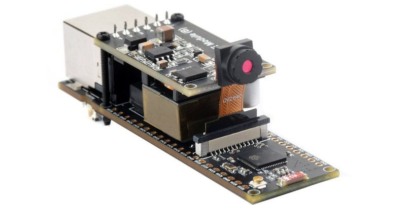
Waveshare has recently released an ESP32-S3-ETH Development Board that combines an ESP32-S3 microcontroller, Ethernet (with optional...
The post Waveshare ESP32-S3-ETH Development Board features Ethernet, PoE, and Camera Interface appeared first on Electronics-Lab.com.
View more at https://www.electronics-lab.com/waveshare-esp32-s3-eth-development-board-features-ethernet-poe-and-camera-interface/.
Credit- ELECTRONICS-LAB. Distributed by Department of EEE, ADBU: https://tinyurl.com/eee-adbu
Curated by Jesif Ahmed
Rikomagic RKM MK42: Compact Mini PC for Retail Kiosks and Digital Signage
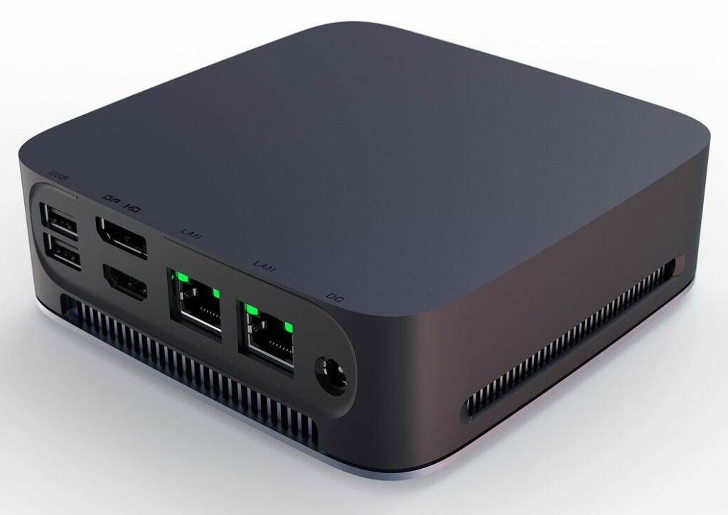
Rikomagic, a Chinese manufacturer specializing in digital signage solutions, has introduced the RKM MK42 Mini PC,...
The post Rikomagic RKM MK42: Compact Mini PC for Retail Kiosks and Digital Signage appeared first on Electronics-Lab.com.
View more at https://www.electronics-lab.com/rikomagic-rkm-mk42-compact-mini-pc-for-retail-kiosks-and-digital-signage/.
Credit- ELECTRONICS-LAB. Distributed by Department of EEE, ADBU: https://tinyurl.com/eee-adbu
Curated by Jesif Ahmed
Palmshell SLiM X4L Mini PC with Intel Processor N100 and Intel UHD Graphics

The Palmshell SLiM X4L is a compact mini PC designed for productivity, presentations, and travel. It...
The post Palmshell SLiM X4L Mini PC with Intel Processor N100 and Intel UHD Graphics appeared first on Electronics-Lab.com.
View more at https://www.electronics-lab.com/palmshell-slim-x4l-mini-pc-with-intel-processor-n100-and-intel-uhd-graphics/.
Credit- ELECTRONICS-LAB. Distributed by Department of EEE, ADBU: https://tinyurl.com/eee-adbu
Curated by Jesif Ahmed
World’s First AI Power Supply With GaN And SiC
The world’s first 8.5kW power supply for AI data centres offers 98% efficiency and new technology. Can it address the industry’s growing power demands? Find out! Navitas Semiconductor has introduced the world’s first 8.5 kW power supply unit (PSU) that uses GaN and SiC technologies to achieve 98% efficiency. Designed for AI and hyperscale data […]
View more at https://www.electronicsforu.com/news/worlds-first-ai-power-supply-with-gan-and-sic.
Credit- EFY. Distributed by Department of EEE, ADBU: https://tinyurl.com/eee-adbu
Curated by Jesif Ahmed
View more at https://www.electronicsforu.com/news/worlds-first-ai-power-supply-with-gan-and-sic.
Credit- EFY. Distributed by Department of EEE, ADBU: https://tinyurl.com/eee-adbu
Curated by Jesif Ahmed
RM-N8MPL Wide-Temp SMARC 2.1 Module with NXP ARM i.MX 8M Plus Processor
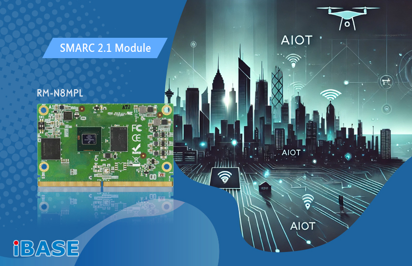
IBASE Technology Inc., a leading manufacturer of embedded motherboards and edge computers, rolls out the RM-N8MPL,...
The post RM-N8MPL Wide-Temp SMARC 2.1 Module with NXP ARM i.MX 8M Plus Processor appeared first on Electronics-Lab.com.
View more at https://www.electronics-lab.com/rm-n8mpl-wide-temp-smarc-2-1-module-with-nxp-arm-i-mx-8m-plus-processor/.
Credit- ELECTRONICS-LAB. Distributed by Department of EEE, ADBU: https://tinyurl.com/eee-adbu
Curated by Jesif Ahmed
Wireless Sensor For Plant Monitoring
A low-cost wireless sensor for plants. Real-time data on plant health, innovative agriculture, better monitoring than expensive methods… Could this be the future of farming? Researchers from the Graduate School of Life Sciences and the Department of Electronic Engineering at Tohoku University have developed a low-cost wireless plant sensor, priced at “a few tens of […]
The post Wireless Sensor For Plant Monitoring first appeared on Electronics For You.
View more at https://www.electronicsforu.com/news/wireless-sensor-for-plant-monitoring.
Credit- EFY. Distributed by Department of EEE, ADBU: https://tinyurl.com/eee-adbu
Curated by Jesif Ahmed
Once Again, the Entire Island of Cuba Falls Into Darkness as Power Grid Collapses
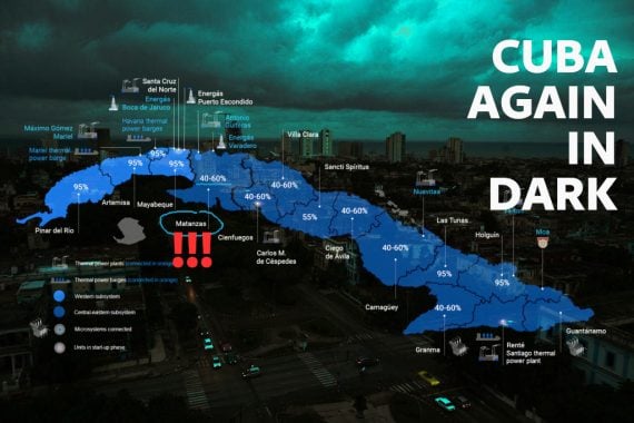
HAVANA, December 4 – Cuba announced the initiation of power restoration following the collapse of the island’s electrical grid, marking the latest incident in a series of statewide blackouts that highlight the deteriorating condition of the country’s power generating infrastructure.... Read more
The post Once Again, the Entire Island of Cuba Falls Into Darkness as Power Grid Collapses appeared first on EEP - Electrical Engineering Portal.
View more at: https://electrical-engineering-portal.com/again-entire-island-of-cuba-falls-into-darkness-power-grid-collapses Credit- EEE - Electrical Engineering Portal. Distributed by Department of EEE, ADBU: https://tinyurl.com/eee-adbu
Curated by Jesif Ahmed.
Robots With Energy-Efficient Movement
The robot dog that trots and hops like nature intended, thanks to groundbreaking research on intrinsic dynamics. Humans and animals achieve exceptional energy efficiency in movement by harnessing the natural oscillation patterns of their bodies—effortlessly and without conscious thought. Now, researchers at the Technical University of Munich (TUM) have developed a groundbreaking tool that applies […]
View more at https://www.electronicsforu.com/news/robots-with-energy-efficient-movement.
Credit- EFY. Distributed by Department of EEE, ADBU: https://tinyurl.com/eee-adbu
Curated by Jesif Ahmed
View more at https://www.electronicsforu.com/news/robots-with-energy-efficient-movement.
Credit- EFY. Distributed by Department of EEE, ADBU: https://tinyurl.com/eee-adbu
Curated by Jesif Ahmed
Pimoroni’s New Clipper HAT Mini Simplifies 4G LTE for Remote Raspberry Pi Projects
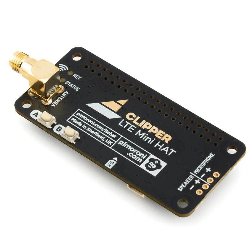
Pimoroni has newly developed the Clipper HAT Mini, an LTE 4G module designed for Raspberry Pi,...
The post Pimoroni’s New Clipper HAT Mini Simplifies 4G LTE for Remote Raspberry Pi Projects appeared first on Electronics-Lab.com.
View more at https://www.electronics-lab.com/pimoronis-new-clipper-hat-mini-simplifies-4g-lte-for-remote-raspberry-pi-projects/.
Credit- ELECTRONICS-LAB. Distributed by Department of EEE, ADBU: https://tinyurl.com/eee-adbu
Curated by Jesif Ahmed
ESP32-S3 1.91-inch AMOLED Board with ESP32-S3R8, RM67162 Driver, and FT3168 Touch Controller
The ESP32-S3 1.91-inch AMOLED development board is designed for rapid prototyping of IoT and portable applications....
The post ESP32-S3 1.91-inch AMOLED Board with ESP32-S3R8, RM67162 Driver, and FT3168 Touch Controller appeared first on Electronics-Lab.com.
View more at https://www.electronics-lab.com/esp32-s3-1-91-inch-amoled-board-with-esp32-s3r8-rm67162-driver-and-ft3168-touch-controller/.
Credit- ELECTRONICS-LAB. Distributed by Department of EEE, ADBU: https://tinyurl.com/eee-adbu
Curated by Jesif Ahmed
Hydrovoltaic Cell Generates Power Without Sunlight Or Water
Engineers from China have developed a unique hydrovoltaic cell capable of generating electricity in extreme conditions with minimal resources. An innovative hydrovoltaic cell has been developed by engineers at the Chinese Academy of Sciences, China offering a solution to generate electricity without requiring sunlight or significant amounts of water. The research introduces the hermetic hydrovoltaic […]
View more at https://www.electronicsforu.com/news/hydrovoltaic-cell-generates-power-without-sunlight-or-water.
Credit- EFY. Distributed by Department of EEE, ADBU: https://tinyurl.com/eee-adbu
Curated by Jesif Ahmed
View more at https://www.electronicsforu.com/news/hydrovoltaic-cell-generates-power-without-sunlight-or-water.
Credit- EFY. Distributed by Department of EEE, ADBU: https://tinyurl.com/eee-adbu
Curated by Jesif Ahmed
“GaN Adaptors Are Smaller, More Powerful, And More Efficient, Offering Up To 95% Efficiency Compared To 80-85% In Silicon Ones” – Subhendu S. Satpathy, CEO, Mokkomotto
What challenges arise when designing electronic products with GaN technology? Subhendu S. Satpathy of Mokkomotto, creator of a 65W GaN charger for all devices, shares his insight with EFY’s Nidhi Agarwal. Q. What are the benefits of using GaN instead of silicon in power adaptors? A. Power adaptors used to vary for each device due […]
View more at https://www.electronicsforu.com/technology-trends/gan-adaptors-are-smaller-more-powerful-efficient-offering-up-to-95-efficiency.
Credit- EFY. Distributed by Department of EEE, ADBU: https://tinyurl.com/eee-adbu
Curated by Jesif Ahmed
View more at https://www.electronicsforu.com/technology-trends/gan-adaptors-are-smaller-more-powerful-efficient-offering-up-to-95-efficiency.
Credit- EFY. Distributed by Department of EEE, ADBU: https://tinyurl.com/eee-adbu
Curated by Jesif Ahmed
“SEMI Is Actively Working With Indian Universities, Institutions To Create India’s Semiconductor Academy” – Ajit Manocha, President of SEMI
India’s semiconductor industry is expected to face a significant talent shortfall, with a projected shortage of 250,000 to 300,000 professionals by 2027. In an insightful conversation, Ajit Manocha, President of Semiconductor Equipment and Materials International (SEMI), revealed to EFY’s Nijhum Rudra and Akanksha Sondhi Gaur, that while the country produces nearly a million STEM graduates […]
View more at https://www.electronicsforu.com/technology-trends/semi-actively-working-with-indian-universities-institutions-create-india-semiconductor-academy.
Credit- EFY. Distributed by Department of EEE, ADBU: https://tinyurl.com/eee-adbu
Curated by Jesif Ahmed
View more at https://www.electronicsforu.com/technology-trends/semi-actively-working-with-indian-universities-institutions-create-india-semiconductor-academy.
Credit- EFY. Distributed by Department of EEE, ADBU: https://tinyurl.com/eee-adbu
Curated by Jesif Ahmed
Liquid Cooled Server Slashes Energy Consumption by 40%
A unique liquid cooled server makes AI applications more efficient, high performance and sustainable across diverse environments. The company of precision liquid cooling (PLC), ‘Iceotope’ launched a liquid cooled server, the ‘KUL AI’, marking a significant milestone in AI infrastructure. It incorporates the PLC technology which validates the unparalleled thermal management and efficiency in computing-intensive […]
View more at https://www.electronicsforu.com/news/liquid-cooled-server-slashes-energy-consumption-by-40.
Credit- EFY. Distributed by Department of EEE, ADBU: https://tinyurl.com/eee-adbu
Curated by Jesif Ahmed
View more at https://www.electronicsforu.com/news/liquid-cooled-server-slashes-energy-consumption-by-40.
Credit- EFY. Distributed by Department of EEE, ADBU: https://tinyurl.com/eee-adbu
Curated by Jesif Ahmed
Waveshare 11.6-inch Touch Display with IPS Panel for Raspberry Pi and Jetson Boards
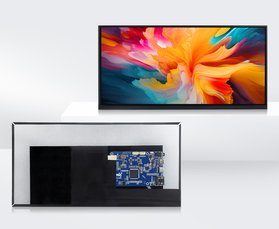
Waveshare has recently launched an 11.6-inch Capacitive Touch Display with in-cell technology, a 1768×828 resolution, and...
The post Waveshare 11.6-inch Touch Display with IPS Panel for Raspberry Pi and Jetson Boards appeared first on Electronics-Lab.com.
View more at https://www.electronics-lab.com/waveshare-11-6-inch-touch-display-with-ips-panel-for-raspberry-pi-and-jetson-boards/.
Credit- ELECTRONICS-LAB. Distributed by Department of EEE, ADBU: https://tinyurl.com/eee-adbu
Curated by Jesif Ahmed
Multi Board Synchronization on RFSoC Board & Systems Demo
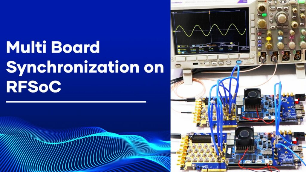
The ZynqTM UltraScale+TM RFSoC architecture integrates FPGA fabric with flexibility and the architecture to support direct RF-sampling,...
The post Multi Board Synchronization on RFSoC Board & Systems Demo appeared first on Electronics-Lab.com.
View more at https://www.electronics-lab.com/multi-board-synchronization-on-rfsoc-board-systems-demo/.
Credit- ELECTRONICS-LAB. Distributed by Department of EEE, ADBU: https://tinyurl.com/eee-adbu
Curated by Jesif Ahmed
JOB: Project Assistant At Amritapuri Campus In Kollam
APPLY HERE Location: Kollam Qualification B.Tech in Electronics & Communication Engineering/ Electronics & Instrumentation / Electrical & Electronics Engineering. Job Description & Responsibilities Skills Required Numbers: 2 Last Date to Apply: 15 December 2024
View more at https://www.electronicsforu.com/career/project-assistant-amritapuri-campus-kollam.
Credit- EFY. Distributed by Department of EEE, ADBU: https://tinyurl.com/eee-adbu
Curated by Jesif Ahmed
View more at https://www.electronicsforu.com/career/project-assistant-amritapuri-campus-kollam.
Credit- EFY. Distributed by Department of EEE, ADBU: https://tinyurl.com/eee-adbu
Curated by Jesif Ahmed
Unified Testing Solution For Wireless Technology
A partnership improves over-the-air (OTA) testing to meet new-tech wireless demands, covering 5G, Wi-Fi 7, and beyond. Rohde & Schwarz and ETS-Lindgren have expanded their collaboration to develop over-the-air (OTA) testing solutions for emerging wireless technologies. The integration of Rohde & Schwarz’s CMX500 signalling tester and SMBV100B vector signal generator into ETS-Lindgren’s EMQuestTM software signifies […]
View more at https://www.electronicsforu.com/news/unified-testing-solution-for-wireless-technology.
Credit- EFY. Distributed by Department of EEE, ADBU: https://tinyurl.com/eee-adbu
Curated by Jesif Ahmed
View more at https://www.electronicsforu.com/news/unified-testing-solution-for-wireless-technology.
Credit- EFY. Distributed by Department of EEE, ADBU: https://tinyurl.com/eee-adbu
Curated by Jesif Ahmed
“Wi-Fi 6 Primarily Focuses On Improving Network Efficiency Rather Than Boosting Data Rates” – Sivaram Trikutam From Infineon Technologies
As Wi-Fi 6 evolve, Wi-Fi 7 is ready to take connectivity to new heights. With extraordinary features like multi-link operation, these technologies are set to realign smart homes and IoT. EFY’s Akanksha sits down with Sivaram Trikutam from Infineon Technologies to discuss what’s next… Q: How do IoT devices enhance daily life, and how can […]
View more at https://www.electronicsforu.com/technology-trends/wi-fi-6-primarily-focuses-on-improving-network-efficiency-rather-than-boosting-data-rates.
Credit- EFY. Distributed by Department of EEE, ADBU: https://tinyurl.com/eee-adbu
Curated by Jesif Ahmed
View more at https://www.electronicsforu.com/technology-trends/wi-fi-6-primarily-focuses-on-improving-network-efficiency-rather-than-boosting-data-rates.
Credit- EFY. Distributed by Department of EEE, ADBU: https://tinyurl.com/eee-adbu
Curated by Jesif Ahmed
High-Performance 200V Power MOSFETs
Provides very low resistance, making it easier to design and improving performance in battery storage and power supply systems. Littelfuse, Inc. has announced the addition of the IXTN400N20X4 and IXTN500N20X4 Ultra Junction X4-Class Power MOSFETs to its 200 V X4-Class Ultra Junction MOSFET lineup. These devices offer low on-state resistance, enabling designers to replace multiple […]
View more at https://www.electronicsforu.com/news/high-performance-200v-power-mosfets.
Credit- EFY. Distributed by Department of EEE, ADBU: https://tinyurl.com/eee-adbu
Curated by Jesif Ahmed
View more at https://www.electronicsforu.com/news/high-performance-200v-power-mosfets.
Credit- EFY. Distributed by Department of EEE, ADBU: https://tinyurl.com/eee-adbu
Curated by Jesif Ahmed
Soft Robotics Advancing Delicate And Hard Tasks
Nature inspired innovation done by a South Korean research team can handle soft to tough tasks and even assists in surgery thereby catalysing robotics applications across fields. A team of roboticists and engineers from South Korea, in collaboration with the Max Planck Institute for Intelligent Systems, has developed a soft, X-shaped robot capable of handling […]
View more at https://www.electronicsforu.com/news/soft-robotics-advancing-delicate-and-hard-tasks.
Credit- EFY. Distributed by Department of EEE, ADBU: https://tinyurl.com/eee-adbu
Curated by Jesif Ahmed
View more at https://www.electronicsforu.com/news/soft-robotics-advancing-delicate-and-hard-tasks.
Credit- EFY. Distributed by Department of EEE, ADBU: https://tinyurl.com/eee-adbu
Curated by Jesif Ahmed
Orbbec and NVIDIA Launch Orbbec Perceptor Developer Kit for Autonomous Mobile Robots
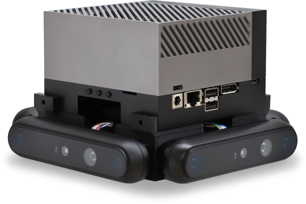
The Orbbec Perceptor Developer Kit (OPDK) is a new out-of-the-box solution for developing autonomous mobile robots (AMRs)....
The post Orbbec and NVIDIA Launch Orbbec Perceptor Developer Kit for Autonomous Mobile Robots appeared first on Electronics-Lab.com.
View more at https://www.electronics-lab.com/orbbec-and-nvidia-launch-orbbec-perceptor-developer-kit-for-autonomous-mobile-robots/.
Credit- ELECTRONICS-LAB. Distributed by Department of EEE, ADBU: https://tinyurl.com/eee-adbu
Curated by Jesif Ahmed
JOB: System Engineer Battery At Alstom In Bengaluru
APPLY HERE Location: Bengaluru Company: Alstom Purpose Of The Job Design and development of battery systems for various Projects/ applications and ensuring safety, reliability, and performance of the battery system meets customer requirements and industry standards. Organisation Reporting Network & Links Responsibilities Knowledge & Experience
View more at https://www.electronicsforu.com/career/system-engineer-battery-alstom-bengaluru.
Credit- EFY. Distributed by Department of EEE, ADBU: https://tinyurl.com/eee-adbu
Curated by Jesif Ahmed
View more at https://www.electronicsforu.com/career/system-engineer-battery-alstom-bengaluru.
Credit- EFY. Distributed by Department of EEE, ADBU: https://tinyurl.com/eee-adbu
Curated by Jesif Ahmed
JOB: Assembly & Test Tech – Level 1 At Honeywell In Gurugram
APPLY HERE Location: Gurugram Company: Honeywell Job Title: Electronics Manufacturing Shopfloor Associate (Assembly Cell) Job Summary The Electronics Manufacturing Shopfloor Associate will be responsible for assembling electronic components and systems within a production line. The role involves precise handling of parts, operating assembly equipment, and ensuring high-quality standards in a fast-paced manufacturing environment. Key Responsibilities […]
View more at https://www.electronicsforu.com/career/assembly-test-tech-level-honeywell-gurugram.
Credit- EFY. Distributed by Department of EEE, ADBU: https://tinyurl.com/eee-adbu
Curated by Jesif Ahmed
View more at https://www.electronicsforu.com/career/assembly-test-tech-level-honeywell-gurugram.
Credit- EFY. Distributed by Department of EEE, ADBU: https://tinyurl.com/eee-adbu
Curated by Jesif Ahmed
JOB: Electrical Designer- Firmware Engineer – STET At Philips In Pune
APPLY HERE Location: Pune Company: Philips You have the opportunity: Manage high impact, complex sustaining & transfer projects that enables Philips to reduce risk, improve profitability, align with Philips’ strategic supply base, and optimize supply chain flexibility. The primary function within this role is to execute engineering activities through the course of fast-paced, high-quality transfer […]
View more at https://www.electronicsforu.com/career/electrical-designer-firmware-engineer-stet-philips-pune.
Credit- EFY. Distributed by Department of EEE, ADBU: https://tinyurl.com/eee-adbu
Curated by Jesif Ahmed
View more at https://www.electronicsforu.com/career/electrical-designer-firmware-engineer-stet-philips-pune.
Credit- EFY. Distributed by Department of EEE, ADBU: https://tinyurl.com/eee-adbu
Curated by Jesif Ahmed
JOB: System Design Engineer At General Electric In Noida and Pallavaram
APPLY HERE Locations: Noida and Pallavaram Company: General Electric Job Description Summary Systems engineering is a cross-functional engineering discipline centered on an approach, mindset, and process. All activities that consider both the business and the technical needs of the customers with the goal of providing a quality product that meets the users needs. The discipline […]
View more at https://www.electronicsforu.com/career/system-design-engineer-general-electric-noida-pallavaram.
Credit- EFY. Distributed by Department of EEE, ADBU: https://tinyurl.com/eee-adbu
Curated by Jesif Ahmed
View more at https://www.electronicsforu.com/career/system-design-engineer-general-electric-noida-pallavaram.
Credit- EFY. Distributed by Department of EEE, ADBU: https://tinyurl.com/eee-adbu
Curated by Jesif Ahmed
Controller For High-Bandwidth Testing And Measurement
A new single-slot compact PXIe controller delivers twice the performance for modern test and measurement applications. A groundbreaking PXIe embedded controller, developed by Pickering Interfaces, UK with next-generation model (43-920-002) significantly advances performance, offering twice the processing power of its predecessor. Designed to support high-bandwidth test and measurement (T&M) applications, the controller is a compact, […]
View more at https://www.electronicsforu.com/news/controller-for-high-bandwidth-testing-and-measurement.
Credit- EFY. Distributed by Department of EEE, ADBU: https://tinyurl.com/eee-adbu
Curated by Jesif Ahmed
View more at https://www.electronicsforu.com/news/controller-for-high-bandwidth-testing-and-measurement.
Credit- EFY. Distributed by Department of EEE, ADBU: https://tinyurl.com/eee-adbu
Curated by Jesif Ahmed
Sensor For Fast Recognition Of People And Objects
The thermal sensor’s wide field of view helps monitor large areas, making it suitable for elderly care, building management, and counting people. Mitsubishi Electric Corporation has launched the MelDIR-brand 80×60-pixel thermal-diode infrared sensor (MIR8060C1), featuring a 100°×73° field of view—more than double the field of view of the company’s current thermal-diode sensors. This expanded field […]
View more at https://www.electronicsforu.com/special/sensor-for-fast-recognition-of-people-and-objects.
Credit- EFY. Distributed by Department of EEE, ADBU: https://tinyurl.com/eee-adbu
Curated by Jesif Ahmed
View more at https://www.electronicsforu.com/special/sensor-for-fast-recognition-of-people-and-objects.
Credit- EFY. Distributed by Department of EEE, ADBU: https://tinyurl.com/eee-adbu
Curated by Jesif Ahmed
JOB: Associate Customer Support Engineer At Tekion In Bengaluru
APPLY HERE Location: Bengaluru Company: Tekion Core Responsibilities Required Skills
View more at https://www.electronicsforu.com/career/associate-customer-support-engineer-tekion-bengaluru.
Credit- EFY. Distributed by Department of EEE, ADBU: https://tinyurl.com/eee-adbu
Curated by Jesif Ahmed
View more at https://www.electronicsforu.com/career/associate-customer-support-engineer-tekion-bengaluru.
Credit- EFY. Distributed by Department of EEE, ADBU: https://tinyurl.com/eee-adbu
Curated by Jesif Ahmed
Compact DC/DC Converter With 97.9% peak efficiency
A converter developed and designed for modern AI and machine learning systems sets new benchmarks in power management, data centre applications. The ‘BMR352’ converter developed by Flex Power Modules, USA is a non-isolated and fully regulated quarter-brick DC/DC converter, offers up to 3kW peak power in a compact size of 58.4mm x 36.8mm x 14.5mm. Supporting […]
View more at https://www.electronicsforu.com/news/compact-dc-dc-converter-with-97-9-peak-efficiency.
Credit- EFY. Distributed by Department of EEE, ADBU: https://tinyurl.com/eee-adbu
Curated by Jesif Ahmed
View more at https://www.electronicsforu.com/news/compact-dc-dc-converter-with-97-9-peak-efficiency.
Credit- EFY. Distributed by Department of EEE, ADBU: https://tinyurl.com/eee-adbu
Curated by Jesif Ahmed
8-Photon Chip Marks Quantum Leap
ETRI achieves a milestone in photonic quantum computing with an advanced qubit manipulation leading to development of quantum technologies Electronics and telecommunications research institute (ETRI), South Korea has reached a milestone in quantum computing with the development of a photonic quantum circuit chip. Capable of controlling up to eight photons, the chip provides a powerful […]
View more at https://www.electronicsforu.com/news/8-photon-chip-marks-quantum-leap.
Credit- EFY. Distributed by Department of EEE, ADBU: https://tinyurl.com/eee-adbu
Curated by Jesif Ahmed
View more at https://www.electronicsforu.com/news/8-photon-chip-marks-quantum-leap.
Credit- EFY. Distributed by Department of EEE, ADBU: https://tinyurl.com/eee-adbu
Curated by Jesif Ahmed
Synchro Check Schemes: Key Techniques and Considerations for Power System Stability

In power systems, synchronization is a fundamental requirement for connecting two sources of electric power, such as a generator to a grid or between segments of the power network. Ensuring that these sources are aligned in frequency, phase sequence, and... Read more
The post Synchro Check Schemes: Key Techniques and Considerations for Power System Stability appeared first on EEP - Electrical Engineering Portal.
View more at: https://electrical-engineering-portal.com/synchro-check-schemes-key-techniques-considerations Credit- EEE - Electrical Engineering Portal. Distributed by Department of EEE, ADBU: https://tinyurl.com/eee-adbu
Curated by Jesif Ahmed.
Compex Systems Unveils Wi-Fi 7 Modules with Smart Connectors, Enabling Seamless Multi-Link Operation (MLO) Integration on Conventional CPU Platforms

Compex Systems (Compex), a global leader in wireless communication technology, is taking Wi-Fi 7 to new...
The post Compex Systems Unveils Wi-Fi 7 Modules with Smart Connectors, Enabling Seamless Multi-Link Operation (MLO) Integration on Conventional CPU Platforms appeared first on Electronics-Lab.com.
View more at https://www.electronics-lab.com/compex-systems-unveils-wi-fi-7-modules-with-smart-connectors-enabling-seamless-multi-link-operation-mlo-integration-on-conventional-cpu-platforms/.
Credit- ELECTRONICS-LAB. Distributed by Department of EEE, ADBU: https://tinyurl.com/eee-adbu
Curated by Jesif Ahmed
Axiomtek’s CEM710 – High-Performance COM Express® Type 7 Module with Industrial-Grade Temperature for Rugged Edge Computing
Axiomtek – a world-renowned leader relentlessly devoted to the research, development, and manufacture of innovative, highly...
The post Axiomtek’s CEM710 – High-Performance COM Express® Type 7 Module with Industrial-Grade Temperature for Rugged Edge Computing appeared first on Electronics-Lab.com.
View more at https://www.electronics-lab.com/axiomteks-cem710-high-performance-com-express-type-7-module-with-industrial-grade-temperature-for-rugged-edge-computing/.
Credit- ELECTRONICS-LAB. Distributed by Department of EEE, ADBU: https://tinyurl.com/eee-adbu
Curated by Jesif Ahmed
Advanced Entry-Level Oscilloscope With Enhanced Versatility
Its educational tools and compact, multi-functional design make it ideal for lab environments and compact spaces, offering a practical and comprehensive solution for modern testing needs. Rohde & Schwarz has announced its latest entry-level oscilloscope, the R&S RTB 2. This upgrade to the popular R&S RTB2000 was originally introduced in 2017 as the first entry-level […]
View more at https://www.electronicsforu.com/news/advanced-entry-level-oscilloscope-with-enhanced-versatility.
Credit- EFY. Distributed by Department of EEE, ADBU: https://tinyurl.com/eee-adbu
Curated by Jesif Ahmed
View more at https://www.electronicsforu.com/news/advanced-entry-level-oscilloscope-with-enhanced-versatility.
Credit- EFY. Distributed by Department of EEE, ADBU: https://tinyurl.com/eee-adbu
Curated by Jesif Ahmed
Automotive Qualified Dual MOSFET Gate Drivers
Nexperia introduces the advanced gate driver series specifically designed for automotive and industrial applications. Nexperia, Netherlands has launched a new series of gate driver ICs, engineered to drive both high-side and low-side N-channel MOSFETs in half-bridge or synchronous buck configurations. The NGD4300-Q100 is specifically designed for automotive applications, such as electronic power steering and power […]
View more at https://www.electronicsforu.com/news/automotive-qualified-dual-mosfet-gate-drivers.
Credit- EFY. Distributed by Department of EEE, ADBU: https://tinyurl.com/eee-adbu
Curated by Jesif Ahmed
View more at https://www.electronicsforu.com/news/automotive-qualified-dual-mosfet-gate-drivers.
Credit- EFY. Distributed by Department of EEE, ADBU: https://tinyurl.com/eee-adbu
Curated by Jesif Ahmed
Atomic Sensors Tracking Real Time Hyperpolarised Molecules
Researchers from IBEC and ICFO introduces new atomic sensor technology improving MRI imaging for precise, real-time control. Research by scientists at Spain’s Institute for Bioengineering of Catalonia (IBEC) and the Institute of Photonic Sciences (ICFO) has introduced atomic sensors that improve MRI quality control by tracking hyperpolarised molecules in real time. These sensors, based on […]
View more at https://www.electronicsforu.com/news/atomic-sensors-tracking-real-time-hyperpolarised-molecules.
Credit- EFY. Distributed by Department of EEE, ADBU: https://tinyurl.com/eee-adbu
Curated by Jesif Ahmed
View more at https://www.electronicsforu.com/news/atomic-sensors-tracking-real-time-hyperpolarised-molecules.
Credit- EFY. Distributed by Department of EEE, ADBU: https://tinyurl.com/eee-adbu
Curated by Jesif Ahmed
Industry’s First 24Gb GDDR7 DRAM
The industry’s first 24-gigabit DRAM sets new standards with the highest capacity and fastest speed, revolutionizing data centers, AI workstations, and more. Samsung Electronics Co., Ltd. announced the development of the first 24-gigabit (Gb) GDDR7 DRAM, featuring the highest capacity and speed to date in the industry. The product is designed for next-generation applications and […]
View more at https://www.electronicsforu.com/news/industrys-first-24gb-gddr7-dram.
Credit- EFY. Distributed by Department of EEE, ADBU: https://tinyurl.com/eee-adbu
Curated by Jesif Ahmed
View more at https://www.electronicsforu.com/news/industrys-first-24gb-gddr7-dram.
Credit- EFY. Distributed by Department of EEE, ADBU: https://tinyurl.com/eee-adbu
Curated by Jesif Ahmed
Fundamentals Of Power Integrity In Low Power Electrical Design
This article discusses the electrical power(s) routed on the PCB and its Integrity down the road as it propagates from VRM to Device, aka Source to Load. Key Takeaways Introduction With the growing demand for faster and more efficient Hardware, particularly in the dynamic environments of consumer electronics, AI/ML, data centers, edge computing, and telecom/networking […]
View more at https://www.electronicsforu.com/technology-trends/fundamentals-of-power-integrity-in-low-power-electrical-design.
Credit- EFY. Distributed by Department of EEE, ADBU: https://tinyurl.com/eee-adbu
Curated by Jesif Ahmed
View more at https://www.electronicsforu.com/technology-trends/fundamentals-of-power-integrity-in-low-power-electrical-design.
Credit- EFY. Distributed by Department of EEE, ADBU: https://tinyurl.com/eee-adbu
Curated by Jesif Ahmed
3D Integration Technique Enhances Near-Sensor Computing
The chip, featuring both chemitransistors and memtransistors, demonstrates potential for precise chemical classification. Researchers at Pennsylvania State University have developed compact near-sensor computing chips using a method known as monolithic 3D (M3D) integration, which enables transistors to be constructed layer by layer on the same substrate. This approach is gaining traction in the semiconductor industry […]
View more at https://www.electronicsforu.com/news/new-products/3d-integration-technique-enhances-near-sensor-computing.
Credit- EFY. Distributed by Department of EEE, ADBU: https://tinyurl.com/eee-adbu
Curated by Jesif Ahmed
View more at https://www.electronicsforu.com/news/new-products/3d-integration-technique-enhances-near-sensor-computing.
Credit- EFY. Distributed by Department of EEE, ADBU: https://tinyurl.com/eee-adbu
Curated by Jesif Ahmed
Jetson Orin NX AI Development Kit: High-Performance Edge AI Solution with NVIDIA Ampere GPU and Cortex-A78AE CPU
The Jetson Orin NX AI Development Kit is centered around the Jetson Orin NX module and...
The post Jetson Orin NX AI Development Kit: High-Performance Edge AI Solution with NVIDIA Ampere GPU and Cortex-A78AE CPU appeared first on Electronics-Lab.com.
View more at https://www.electronics-lab.com/jetson-orin-nx-ai-development-kit-high-performance-edge-ai-solution-with-nvidia-ampere-gpu-and-cortex-a78ae-cpu/.
Credit- ELECTRONICS-LAB. Distributed by Department of EEE, ADBU: https://tinyurl.com/eee-adbu
Curated by Jesif Ahmed
Circuit Canvas is A Free Web-based Drawing Tool for Quick Circuit Design and Electronics Schematics
If you just started electronic or you love simulating or building circuits, you have definitely worked...
The post Circuit Canvas is A Free Web-based Drawing Tool for Quick Circuit Design and Electronics Schematics appeared first on Electronics-Lab.com.
View more at https://www.electronics-lab.com/circuit-canvas-is-a-free-web-based-drawing-tool-for-quick-circuit-design-and-electronics-schematics/.
Credit- ELECTRONICS-LAB. Distributed by Department of EEE, ADBU: https://tinyurl.com/eee-adbu
Curated by Jesif Ahmed
NXP i.MX RT700 AI Crossover MCU also features eIQ Neutron NPU and DSPs
NXP has recently announced NXP i.MX RT700 RT700 AI crossover MCU is designed for devices that require...
The post NXP i.MX RT700 AI Crossover MCU also features eIQ Neutron NPU and DSPs appeared first on Electronics-Lab.com.
View more at https://www.electronics-lab.com/nxp-i-mx-rt700-ai-crossover-mcu-also-features-eiq-neutron-npu-and-dsps/.
Credit- ELECTRONICS-LAB. Distributed by Department of EEE, ADBU: https://tinyurl.com/eee-adbu
Curated by Jesif Ahmed
Wearable Device Enhances Senses With Skin Feedback
The wearable device uses skin-stimulation technology to provide feedback, helping with navigation, balance, and assisting those with visual impairments or prosthetics. A team of engineers led by Northwestern University has created a new wearable device that stimulates the skin to deliver a range of complex sensations. This thin, flexible device adheres comfortably to the skin, […]
View more at https://www.electronicsforu.com/news/wearable-device-enhances-senses-with-skin-feedback.
Credit- EFY. Distributed by Department of EEE, ADBU: https://tinyurl.com/eee-adbu
Curated by Jesif Ahmed
View more at https://www.electronicsforu.com/news/wearable-device-enhances-senses-with-skin-feedback.
Credit- EFY. Distributed by Department of EEE, ADBU: https://tinyurl.com/eee-adbu
Curated by Jesif Ahmed
AI-Powered Sensor Ensuring Food Quality
The AI based sensor (artificial tongue) developed by Penn State University (PSU) which can instantly detect food freshness and safety with over 95% accuracy. Researchers at Penn State University, Pennsylvania have developed an AI-driven electronics sensor capable of analysing subtle differences in liquids, significantly advancing food safety and diagnostic applications. This innovative device not only […]
View more at https://www.electronicsforu.com/news/ai-powered-sensor-ensuring-food-quality.
Credit- EFY. Distributed by Department of EEE, ADBU: https://tinyurl.com/eee-adbu
Curated by Jesif Ahmed
View more at https://www.electronicsforu.com/news/ai-powered-sensor-ensuring-food-quality.
Credit- EFY. Distributed by Department of EEE, ADBU: https://tinyurl.com/eee-adbu
Curated by Jesif Ahmed
Memristor Design Makes Computers Smarter
Researchers at Wuhan University have developed new, more effective memristors using special metallic materials. The growing use of AI-based models is increasing demands on the electronics industry for more storage and computational power. Engineers are responding by developing neuromorphic computing systems that often utilize memristors, components that regulate electrical currents and remember past charges, similar […]
View more at https://www.electronicsforu.com/news/memristor-design-makes-computers-smarter.
Credit- EFY. Distributed by Department of EEE, ADBU: https://tinyurl.com/eee-adbu
Curated by Jesif Ahmed
View more at https://www.electronicsforu.com/news/memristor-design-makes-computers-smarter.
Credit- EFY. Distributed by Department of EEE, ADBU: https://tinyurl.com/eee-adbu
Curated by Jesif Ahmed
JOB: Layout Design, Engineer At Synopsys In Bengaluru
APPLY HERE Location: Bengaluru Company: Synopsys You Are You are a highly motivated individual with a passion for layout design and a keen eye for detail. You thrive in a collaborative environment and are excited by the opportunity to work on cutting-edge technology. You have a strong background in semiconductor design and are proficient in […]
View more at https://www.electronicsforu.com/career/layout-design-engineer-synopsys-bengaluru.
Credit- EFY. Distributed by Department of EEE, ADBU: https://tinyurl.com/eee-adbu
Curated by Jesif Ahmed
View more at https://www.electronicsforu.com/career/layout-design-engineer-synopsys-bengaluru.
Credit- EFY. Distributed by Department of EEE, ADBU: https://tinyurl.com/eee-adbu
Curated by Jesif Ahmed
AI Co-Pilot Transforming EdgeAI Accessibility
SmartSoC Solutions has launched an AI-driven co-pilot ‘Hinton’ that offers enterprises intuitive, voice-guided tools for managing AI on edge devices. Hinton launched by Bengaluru based SmartSoC AI studio provides a suite of tools spanning computer vision, generative AI (GenAI), and natural language processing (NLP), making it ideal for industries seeking to integrate AI in real-time […]
View more at https://www.electronicsforu.com/news/ai-co-pilot-transforming-edgeai-accessibility.
Credit- EFY. Distributed by Department of EEE, ADBU: https://tinyurl.com/eee-adbu
Curated by Jesif Ahmed
View more at https://www.electronicsforu.com/news/ai-co-pilot-transforming-edgeai-accessibility.
Credit- EFY. Distributed by Department of EEE, ADBU: https://tinyurl.com/eee-adbu
Curated by Jesif Ahmed
Quantum Driven Transistors For Ultra-Efficient Electronics
3D transistors utilising ultrathin materials and quantum mechanics to create devices that operate at ultra-low voltages that promise faster, more powerful electronics, paving the way for a new era in energy-efficient computing. Silicon transistors are the backbone of modern electronics, powering everything from smartphones to AI-driven devices by amplifying and switching electronic signals. However, traditional […]
View more at https://www.electronicsforu.com/news/quantum-driven-transistors-for-ultra-efficient-electronics.
Credit- EFY. Distributed by Department of EEE, ADBU: https://tinyurl.com/eee-adbu
Curated by Jesif Ahmed
View more at https://www.electronicsforu.com/news/quantum-driven-transistors-for-ultra-efficient-electronics.
Credit- EFY. Distributed by Department of EEE, ADBU: https://tinyurl.com/eee-adbu
Curated by Jesif Ahmed
Sensor Targets Food Antioxidants
Researchers have recently developed an electrochemical sensor for detecting tert-butylhydroquinone (TBHQ), a synthetic antioxidant frequently used in food preservation. The new sensor, developed by a research team from Hunan City University & Xiangtan University, China provides a sensitive, efficient, and potentially more accessible approach to food antioxidants- TBHQ detection, advancing food quality analysis methods which […]
View more at https://www.electronicsforu.com/news/sensor-targets-food-antioxidants.
Credit- EFY. Distributed by Department of EEE, ADBU: https://tinyurl.com/eee-adbu
Curated by Jesif Ahmed
View more at https://www.electronicsforu.com/news/sensor-targets-food-antioxidants.
Credit- EFY. Distributed by Department of EEE, ADBU: https://tinyurl.com/eee-adbu
Curated by Jesif Ahmed
Thermal Printing Reference Design
The design helps control thermal printers effectively, ensuring accurate printing even when the operating system is unpredictable. Thermal printing is a critical technology widely used across various industries because it produces high-quality prints quickly and efficiently. Renowned for its speed, thermal printers significantly outpace traditional inkjet or laser printers, making them ideal for fast-paced environments […]
View more at https://www.electronicsforu.com/electronics-projects/thermal-printing-reference-design.
Credit- EFY. Distributed by Department of EEE, ADBU: https://tinyurl.com/eee-adbu
Curated by Jesif Ahmed
View more at https://www.electronicsforu.com/electronics-projects/thermal-printing-reference-design.
Credit- EFY. Distributed by Department of EEE, ADBU: https://tinyurl.com/eee-adbu
Curated by Jesif Ahmed
Portable Power Tool Reference Design
It meets the needs of DIY users and professionals alike by combining advanced motor control, optimized power management, and versatile connectivity in a robust, high-performance package. A growing interest in DIY projects has fueled the increasing popularity of portable power tools, driving demand for compact, high-performance, and cost-effective tools with advanced technology. Toolmakers continually innovate, […]
View more at https://www.electronicsforu.com/electronics-projects/portable-power-tool-reference-design.
Credit- EFY. Distributed by Department of EEE, ADBU: https://tinyurl.com/eee-adbu
Curated by Jesif Ahmed
View more at https://www.electronicsforu.com/electronics-projects/portable-power-tool-reference-design.
Credit- EFY. Distributed by Department of EEE, ADBU: https://tinyurl.com/eee-adbu
Curated by Jesif Ahmed
Gate Driver IC Enhances Safety In Automotive
The gate driver IC for 12V BLDC motors has been launched for applications like brake-by-wire and steer-by-wire systems, which meet top automotive safety standards. Infineon Technologies AG has launched the MOTIX TLE9189 gate driver IC for 12 V brushless DC (BLDC) motors in safety-critical applications. This three-phase gate driver IC meets the needs of motor […]
View more at https://www.electronicsforu.com/news/gate-driver-ic-enhances-safety-in-automotive.
Credit- EFY. Distributed by Department of EEE, ADBU: https://tinyurl.com/eee-adbu
Curated by Jesif Ahmed
View more at https://www.electronicsforu.com/news/gate-driver-ic-enhances-safety-in-automotive.
Credit- EFY. Distributed by Department of EEE, ADBU: https://tinyurl.com/eee-adbu
Curated by Jesif Ahmed
Advancements In TOPCon Solar Cells
Researchers at the Chinese Academy of Sciences & Zhejiang University have developed a TOPCon bottom cell that improves perovskite solar cells, making them more efficient. Silicon solar cells are gaining significant traction in the photovoltaic industry, drawing widespread interest due to their promising future. Specifically, silicon solar cells equipped with tunnel oxide passivating contact (TOPCon) […]
View more at https://www.electronicsforu.com/news/advancements-in-topcon-solar-cells.
Credit- EFY. Distributed by Department of EEE, ADBU: https://tinyurl.com/eee-adbu
Curated by Jesif Ahmed
View more at https://www.electronicsforu.com/news/advancements-in-topcon-solar-cells.
Credit- EFY. Distributed by Department of EEE, ADBU: https://tinyurl.com/eee-adbu
Curated by Jesif Ahmed
Arduino-based Sewer Drain Shield for Smart Cities
Drainage systems are vital for storm water management but often transport pollutants, especially plastics, to rivers and oceans, harming ecosystems. Traditional sewer cleaning methods include manual labour, hydraulic flushing, and chemical cleaners. Instead, this DIY sewer drain shield system, combining ultrasonic sensors, GSM modules, nets, and PVC pipes, reduces debris entering drainage systems, thus ensuring […]
View more at https://www.electronicsforu.com/electronics-projects/arduino-sewer-drain-shield.
Credit- EFY. Distributed by Department of EEE, ADBU: https://tinyurl.com/eee-adbu
Curated by Jesif Ahmed
View more at https://www.electronicsforu.com/electronics-projects/arduino-sewer-drain-shield.
Credit- EFY. Distributed by Department of EEE, ADBU: https://tinyurl.com/eee-adbu
Curated by Jesif Ahmed
Subscribe to:
Posts (Atom)