Digital Synchronous Counter – Types, Working & Applications

Digital Synchronous Counter – Types & Applications

What is Digital Counter?

A digital binary counter is a device used for counting binary numbers. Digital counters mainly use flip-flops and some combinational circuits for special features.

As we know flip-flop operates on clock pulses. So the counter will count up or down using these pulses. The time period of clock signal will affect time delay in the counter. So this counter can also be modified into a timepiece given the clock signal has a time period of 1 second.

What is Synchronous Counter?

As the name implies, the synchronous counter contains flip-flops which are all in sync with each other i.e. their clock inputs are connected together and are triggered by the same external clock signal. This implies that all the flip-flops update its value at the same time.

Types of Synchronous Counters

There are two types of counters.

Synchronous counters and Asynchronous Counters. The synchronous counter has many types. Some of them are given below.

  • Up-Counter
  • Down Counter
  • Up/Down Counter
  • BCD Counter

Up Counter

This synchronous counter counts up from 0 to 15 (4-bit counter). Up counter can be designed using T-flip flop (JK-flip flop with common input) & D-flip flop. Both of these flip-flops have a different configuration.

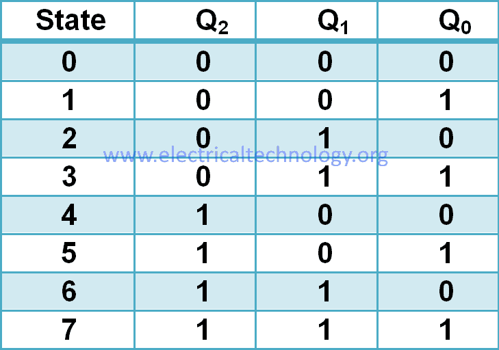
Consider a 3-bit counter with each bit count represented by Q0, Q1, Q2­as the outputs of Flip-flops FF0, FF1, FF2 respectively.Then the state table would be:
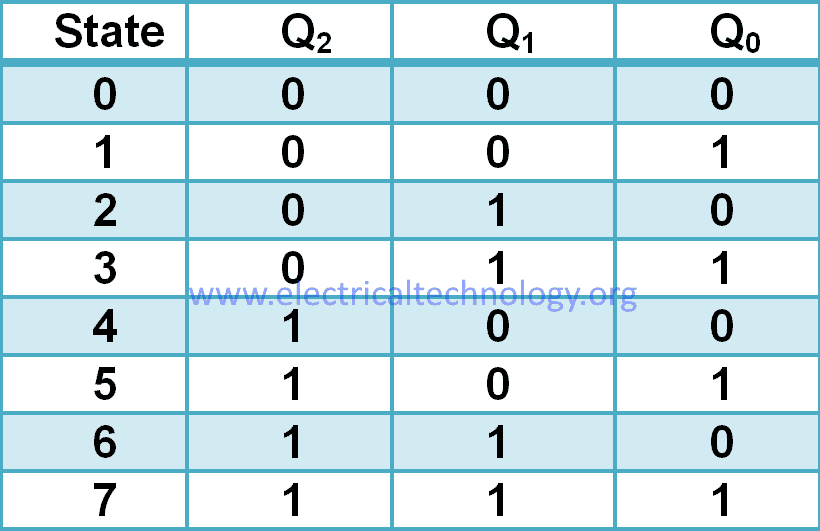
up counter truth table

The counter is a memory device. It means it has previous & next states.

Design Using T-Flip Flop

T-Flip flop toggles it state when input = 1 and holds its state when input= 0.

According to the state table of up-counter

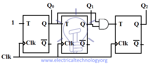
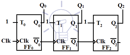
Q0 ­is continuously toggling so the input to the FF0 will be permanent 1. i.e. T0 = 1.

Q1 toggles its state when the previous state is Q­0 = 1. So the input to FF1 will be the output of FF0 i.e. T1 = Q0

Q2 toggles when both Q0 & Q1 are 1. So the input to FF2 will be the AND of outputs of FF0 & FF1 i.e. T2 = Q0 & Q1.

The schematic for Up-counter using T-flip flops is given below.Up-counter using T-flip flops - Synchronous Counter
Design Using D-Flip Flop

D-Flip flop updates its state according to the input applied to it i.e. Q = D. So designing up-counter using D-flip flop is different than a T-flip flop.

According to the state table of up-counter

Q0 is continuously changing so the input to FF0 will be D0 = Q̅0. Because it will toggle the state whenever a clock pulse hits the FF0.

Q1 = 1, when its previous state Q1 &Q0 are not equal & Q1 = 0, when its previous state Q1 &Q0 are equal. That is the same as XOR operation. So D1 = Q1 XOR Q0.

Q2 = 1, when in its previous state the AND of Q1 & Q0 is not equal to Q2. Q2 = 0, when in its previous state the AND of Q1 & Q0 is equal to Q2.So D2 = Q2 XNOR (Q1& Q0)

Schematic of Synchronous Up-counter using D-flip flop is given in the figure below.
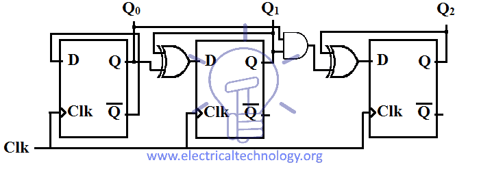
Synchronous-Up-counter-using-D-flip-flop

Down Counter

Down counter counts in descending order from 15 to 0 (4-bit counter). Down counter can also be designed using T-flip flop and D-flip flop.

Consider 3-bit counter with each bit represented by Q0, Q1, Q2as the outputs of flip-flops FF0, FF1, FF2 respectively. The state table for down counter is given below:
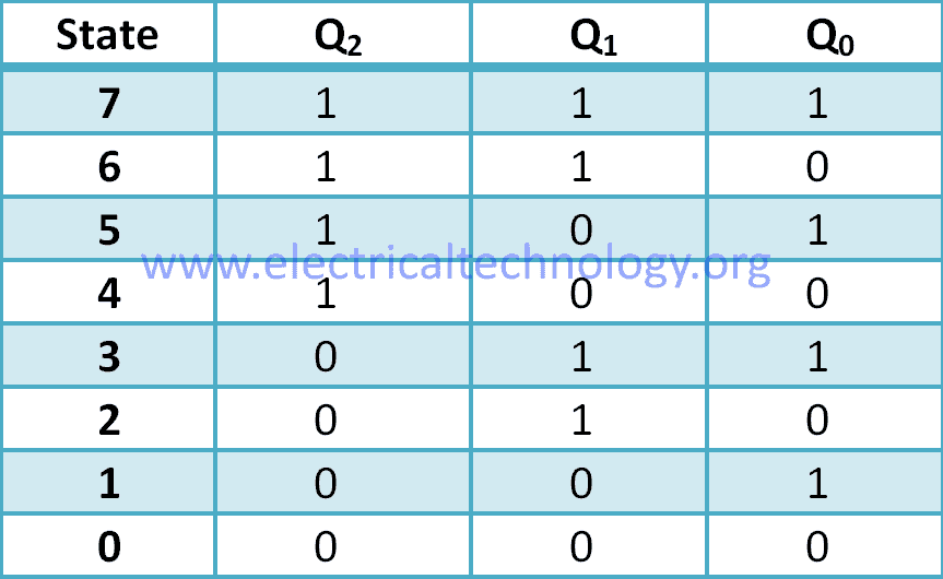
down counter state table

Design Using T-Flip Flop

T-flip flop toggles its state when T-input = 1 & hold its state when T=0.

According to the state table of Down-counter

Q0 ­is continuously toggling so the input to the FF0 will be permanent 1. i.e. T0 = 1.

Q1 toggles its state when the previous state is Q­0 = 0. So the input to FF1 will be the complemented output of FF0 i.e. T1 = Q̅0

Q2 toggles when both Q0 & Q1 are 0. So the input to FF2 will be the AND of complemented outputs of FF0 & FF1 i.e. T2 = Q̅0 & Q̅1.

The schematic for Down-counter using T-flip flops is given below
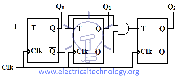
Down-counter-using-T-flip-flops

Design Using D-Flip Flop

D-flip flop updates its states according to the input D i.e. Q = D. so its design is different than T-flip flop design.

According to the state table of down-counter

Q0 is continuously changing so the input to FF0 will be D0 = Q̅0. Because it will toggle the state whenever a clock pulse hits the FF0.

Q1 = 1, when its previous state Q1 &Q0 are equal & Q1 = 0, when its previous state Q1 &Q0 are not equal. That is the same as XNOR operation. So D1 = Q1 XNOR Q0.

Q2 = 1, when in its previous state the OR of Q1 & Q0 is equal to Q2. Q2 = 0, when in its previous state the OR of Q1 & Q0 is equal to Q2.So D2 = Q2 XNOR (Q1 + Q0)

Schematic of Synchronous Down-counter using D-flip flops is given in the figure below.
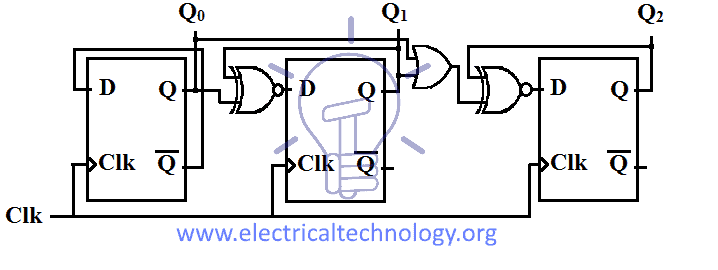
Schematic-of-Synchronous-Down-counter-using-D-flip-flops

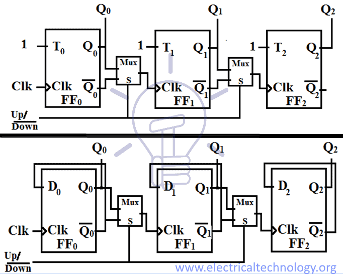
Up/Down Counter

This counter has two modes of counting i.e. up counting and down counting. There is a mode switch which switches between the two modes of the counter. When the mode M = 0 it counts up & when mode M = 1 then it counts down.

This Counter combines up-counter & down-counter using 2_1 mux. The Mux selects one counter using the select switch which is the mode switch.

Design Using T-Flip Flop
Up-Down-counter-Design-using-T-Flip-flop

We combine up & down counter of T-flip flop into one counter. We used 2_1 Mux for the inputs on each flip-flop except the first one.

When Mode = 0, the upper input will be selected and Up counting will start.

When Mode = 1, the lower input will be selected and down counting will start.

Design using D-Flip Flop
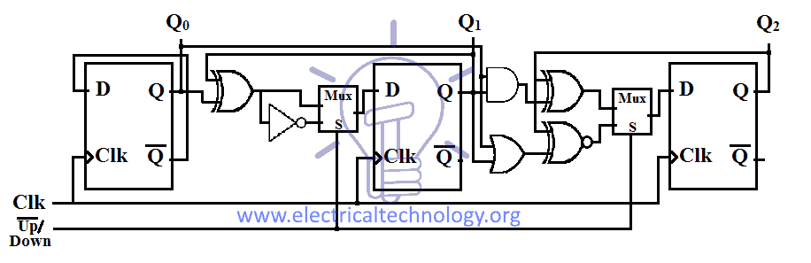
Up-Down-counter-Design-using-D-Flip-flop

We use 2_1 Muxes to Combining Up & down counter using D-Flip flop into a single counter. The inputs to each flip-flop are selected by 2_1 Mux which selects the mode of the counting.

BCD Counter

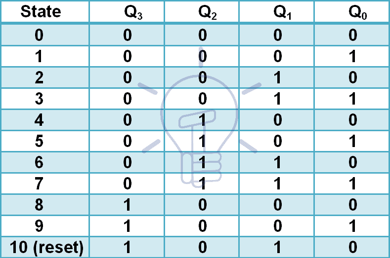
Binary coded decimal (BCD) counter is a modified binary counter with MOD n = 10. MOD is the number of states that a counter can have. Any counter with MOD = 10 is known as decade counter. It has 10 states each representing one of 10 decimal numbers. Which is why it is known as BCD counter. It counts from 0 to 9 and then it resets back to 0.

The default state of BCD counter is 0000 when it reaches decimal count 10 it resets to 0.

Consider Q0, Q1, Q2, Q3as 4 bits of the counter than the state table will be.
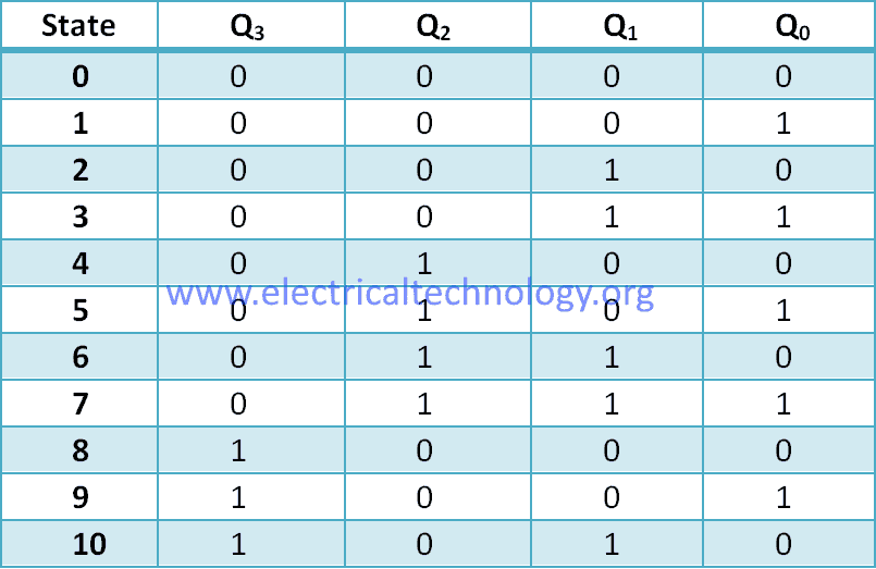
BCD-counter-state-table

BCD counter can be made using T-Flip flop or D-Flip flop.

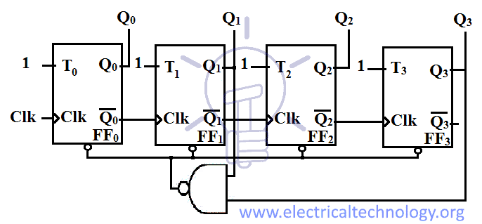
Design using T-Flip Flop

The designing of BCD counter using T-flip flop is same as Up-counter but there is a condition when the count or state reaches to 1010 (decimal 10) it will clear all the flip-flops to default state 0000 (decimal 0).

Flip flops normally have active low clear. So we have to apply combinational circuit to automatically reset the circuit upon reaching 1010 state. The combinational circuit should produce ‘0’ to clear the flip-flops.

NAND gate produces logic 0 when all its inputs are true so whenever Q3 & Q1 = 1, NAND will produce 0. Thus

Clear = (Q3& Q1)’

Schematic of BCD counter using T-flip flops is given below:
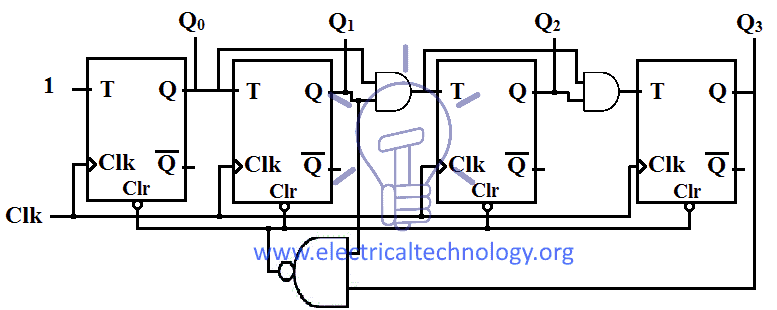
Schematic-of-BCD-counter-using-T-flip-flops

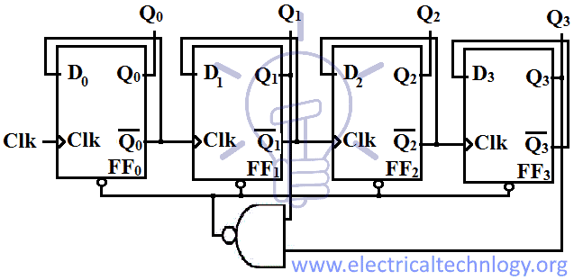
Design Using D-Flip Flop

BCD counter using D-flip flop is a modified D-flip flop’s Up-counter. The modification it needs is the auto-reset function upon reaching the state 1010 which is decimal 10.

Reset function will clear the flip-flop to default state 0000 to start the count again from 0.

The combinational circuit for reset function is the same as in T-flip flop BCD counter.

Schematic of BCD counter using D-flip flop is given below.
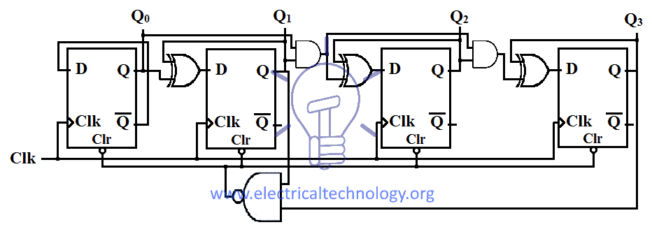
Schematic-of-BCD-counter-using-D-flip-flop

BCD counters are used in digital clock and event counting.


Advantages / Disadvantages of Synchronous Counters

  • Very easy to design this circuit because we may set the same clock pulse for all gates.
  • Less likely to end up in erroneous states.
  • They are faster as the the propagation delay are small as compared to asynchronous counters.
  • There are no counting errors as compared to asynchronous counters.
  • Performance is much better, liable and portable circuit.

Applications of Synchronous Counters

As the name suggest, Synchronous counters perform “counting” such as time and electronic pulses (external source like infrared light). They are widely used in lots of other designs as well such as processors, calculators, real time clock etc. Some common uses and application of synchronous counters are follow:

  • Alarm Clock, Set AC Timer, Set time in camera to take the picture, flashing light indicator in automobiles, car parking control etc.
  • Counting the time allotted for special process or event by the scheduler.
  • The UP/DOWN counter can be used as a self-reversing counter.
  • It is also used as clock divider circuit.
  • The parallel load feature can be used to preset the counter for some initial count.
  • Commons used in home appliances like washing machine, microwave own, Time schedule led indicator, key board controller etc.
  • They are also used in machine moving control.
  • Mostly used in digital clocks and multiplexing circuits.
  • They are used to generate saw-tooth waveform (Stair case voltage)
  • It is also used in digital to analog converters.

You may also read:

The post Digital Synchronous Counter – Types, Working & Applications appeared first on Electrical Technology.


May 08, 2018 at 07:30PM by Department of EEE, ADBU: https://ift.tt/2AyIRVT

Digital Asynchronous Counter (Ripple Counter) & Types

Types of Digital Asynchronous Counter (Ripple Counter)

What is Counter ?

A digital binary counter is a device used for counting binary numbers. Digital counters mainly use flip-flops and some combinational circuits for special features.

What is Asynchronous Counter or Ripple Counter?

The counter in which external clock is only given to the first Flip-flop & the succeeding Flip-flops are clocked by the output of the preceding flip-flop is called asynchronous counter or ripple counter. The name ripple counter is because the clock signal ripples its way from the first stage of Flip-flops to the last stage.

Types of Asynchronous Counters

There are two types of counters.

Synchronous counters and Asynchronous Counters. The asynchronous counter has many types. Some of them are given below.

  • Up-Counter
  • Down Counter
  • Ripple Up/Down Counter
  • Ripple BCD Counter

Up-Counter

Ripple up-counter starts counting from 0 and counts up to its maximum range. Its range depends on the number of flip-flop being used.

Ripple up-counter can be made using T-Flip flop and D-Flip flop.Designing of counters using flip-flops differs from each other with the type of flip-flop being used.  

Consider a 3-bit counter with Q0, Q1, Q2 as the output of Flip-flops FF0, FF1, FF2 respectively. The state table for the 3-bit counter is given below:

3-bit counter Truth Table

Design Using T-Flip Flop

T-Flip flop toggles its state when its input T = 1. In Ripple counter using T-flip flop, input to all stages (flip-flop) is T = 1. The only thing which is not common in these stages is the clock signal. It means that the flip-flop will only toggle when the clock pulse hits the flip-flop. So the clock signal of the succeeding T-Flip flops has to be managed in such way that the Flip-flop toggles when they are supposed to.

Suppose positive edge sensitive T-flip flop is being used in the design.According to the state table of up-counter,

Q0 is toggling continuously so the external clock will be fed to the flip-flop FF0. It will toggle the Q0 upon the positive edge of the clock signal.

Q1 toggles when Q0 goes from 1 to 0. It means that the Negative edge of Q0 toggles Q1. So we can use Q0 as the clock input for FF1. We are using Positive edge triggered flip-flops so we will use complemented Q0 as the clock input for FF1.

Q2 toggles when Q1 goes from 1 to 0 (negative edge).  This can also be used as a clock signal for FF2.Since we are using positive edge sensitive flip-flops, we need the complemented Q1 as the clock input for FF2

Schematic of ripple Up-counter using T-flip flop is given in the figure below.

Schematic of ripple Up-counter using T-flip flop Asynchronous Counter

Design Using D-Flip Flop

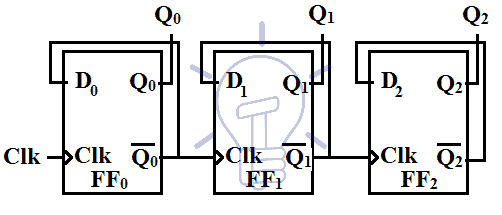
Data or D-flip flop uploads input D as its output state Q upon clock edge. i.e Q = D. D-flip flop can also be used to implement Ripple Up-counter.

D-flop flop can be set to toggle its state upon the clock edge if its complemented output is feedback to its input. In such setup, D-flip flop can act as a T-flip flop with input T = 1.

Since the D-flip flop can be set to act as a T-flip flop, we can use the same design of T-flip flop up counter by replacing T-flip flop with D-flip flop. The input of each individual D-flip flop will be connected its complemented output D = Q̅. Whenever the clock edge hits the flip-flop will toggle its state.

The toggling pattern is the same as in the T-flip flop’s up-counter. So the clock signal input should be designed as in the T-flip flop Up-counter.

The schematic of Ripple up-counter using D-flip flop is given in the figure below:

schematic of Ripple up-counter using D-flip flop

Down Counter

This counter counts down numbers from highest possible count to 0 and then resets back from the highest count.

Assume 3 bit down counter with Q0 Q1 Q­2 as outputs of flip-flops FF0 FF1 FF2 respectively. The state table of down-counter is given below:

3-bit counter Truth Table

Design Using T-Flip Flop

Designing of Down-counter is the same as up counter. The only difference is the toggling of the flip-flop. Each flip-flop toggles when its preceding flip-flop’s output goes from 0 to 1. It is opposite of the up-counter.

In up-counter, we used Positive edge sensitive flip-flops and we used Q̅ of preceding flip-flop as the clock signal for these flip-flops. In down-counter case we will use Q as the clock signal.

The schematic for Down-counter using T-flip flop is given below.

Schematic of ripple Up-counter using T-flip flop

Design Using D-flip Flop

Design of Down-counter using D-flip flop is also same as T-flip flop down-counter. The clock signal that is provided to the succeeding Flip-flops in D-flip flop Up-counter will be changed as done in T-flip flop down-counter.

The output of each flip-flop will be fed as a clock input to the succeeding D-flip flops. This will enable the counter to count backward.

The schematic design for ripple down-counter using D-flip flop is given below:

schematic of Ripple up-counter using D-flip flop

Ripple Up/Down Counter

This counter can do both up counting and down counting depending on the mode select switch. Mode select is a switch that selects between up-counting & down-counting. When M=1, the counter will count up and when M=0, the counter will count down.

The difference between the up-counter and down-counter is the clock signal. So we will use 2_1 Mux to select the 2 clock signals.

Schematic of ripple Up/Down counter is given below:

Ripple BCD Counter

BCD (Binary coded decimal) counter is a decade counter which has Mod = 10. Mod means the number of states the counter have. BCD counter counts decimal numbers from 0 to 9 and resets back to default 0. With each clock pulse, the counter counts up a decimal number.

Ripple BCD counter is same as Ripple Up-counter, the only difference is when BCD counter reached to count 10 it resets its flip-flops.

Consider Q0, Q1, Q2, Q3as 4 bits of the counter than the state table for Ripple BCD counter will be.

Ripple BCD counter state table

According to the state table, it is a simple up counter except state 10 as reset state condition.

Whenever the count reaches to state 10 the counter should automatically clear its flip-flops. For this purpose, we need a combinational circuit. Flip-flops have usually active-low clear. To clear all flip-flops the combinational circuit should produce logic ‘0’ when the counter reached state 1010. NAND gate also produces logic ‘0’ when all its inputs are true.

So we will use NAND gate to clear the flip-flop when it reaches to count 10.

Clear = (Q3 AND Q1)’

Ripple BCD counter can be made using T-flip flops or D-flip flops.

Design Using T-Flip Flop

We will use the reset condition for the up-counter T-flip flop to make it BCD counter. It schematic is shown in the figure given below:

schematic using up-counter T-flip flop Ripple to make BCD counter

Design Using D-Flip Flop

We can modify the D-flip flop Up-counter into ripple BCD counter. Essentially these both are the same up counter but BCD counter has a limit of 10 counts. So when up-counter reaches count 10 it should reset to default state which makes it a ripple BCD counter.

Schematic for Ripple BCD counter using D-flip flop is given below:

Schematic for Ripple BCD counter using D-flip flop

Advantages of Asynchronous Counters

  • It can be easily designed by D-flip flop or T-flip flop.
  • It can be used in low speed circuits.
  • It is used as Divide by-n counters.
  • They are also used as Truncated counters. (to design any mod number counters, i.e. Mod 4, Mod 3).

Disadvantages

  • For Re synchronization, extra flip flop are needed.
  • Additional feedback logic is needed to count the sequence of truncated counters (keep in mind that mod is not equal to 2n).
  • The propagation delay of asynchronous counters is very large, while counting large number of bits.
  • Due to propagation delay, counting errors may occur for high clock frequencies.
  • They are slower as compared to synchronous counters.

Applications of Asynchronous Counters

  • They are used as frequency dividers, as divide by “N” counters.
  • They are used for low noise emission and low power applications
  • They are used in designing asynchronous decade counter.
  • It is also used in Ring counter and Johnson counter.
  • Asynchronous counters are used in Mod N ripple counters. i.e. Mod 3, Mod 4, Mod 8, Mod 14, Mod 10 etc.

You may also read:

The post Digital Asynchronous Counter (Ripple Counter) & Types appeared first on Electrical Technology.


May 07, 2018 at 02:08AM by Department of EEE, ADBU: https://ift.tt/2AyIRVT
Ring Counter & Johnson Counter – Construction & Operation

Construction & Working of Ring Counter & Johnson Counter

What is Ring Counter & Johnson Counter?

In our previous post, we have discussed different types of electronic counters in details, to the ring counter, a type of counter in which the output of the last flip-flop is connected as an input to the first flip-flop is known as a Ring counter. The input is shifted between the flip-flops in a ring shape which is why it is known as a Ring counter.

A Ring counter is a synchronous counter. the synchronous counter has a common clock signal that triggers all the Flip-flops at the same time. Ring counter consists of D-flip flops connected in cascade setup with the output of last Flip-flop connected to the input of first Flip-flop. Each flip-flop constitutes a stage.


Difference between Ring Counter & Johnson Counter?

Ring Counter:

This counter is developed by modifying a shift register. The true output of the last flip-flop is fed back directly to the data input of the first flip-flop, thus generating a sequence of pulses. For example, for a D Flip-Flop shift register, the Q output of the last flip-flop is connected to the D input of the first flip-flop. These counters are used in digital system to generate control pulses.

Johnson Counter

Johnson counter is a reverse of Ring Counter. In other words, feedback from the last flip-flop is fed inversely to the data input of the first flip-flop. For example, for a D Flip-Flop shift register, the ~Q output of the last flip-flop is fed to the D input of the first flip-flop. These can be used as Divide by n counters as well.

Types of Ring Counters

There are two types of the Ring counter.

  • A Typical Ring Counter
  • Johnson counter

Typical Ring Counter

A typical 4-bit ring counter is made of D-flip flops or JK-flip flop connected in cascade with the non-complemented output of the last stage connected as an input to the first stage. Ring counter has Mod = n ‘n’ is the number of bits. It means 4-bit ring counter has 4 states.

Ring Counter Truth Table

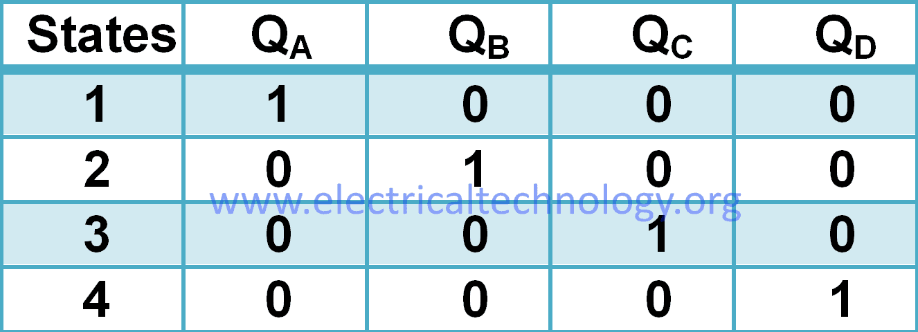
Consider QA, QB, QC, QD as the 4 bits of the ring counter. The truth table for 4-bit ring counter is given below.

4-bit ring counter truth table

In ring counter, logic ‘1’ flows through all stages of the counter. In each state, it flows one bit to the right. When it reaches stage 4, it circulates back to stage1 of the counter.

Working of Ring Counter

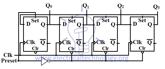
Ring counter’s state needs to be set before the operation. Since ring counter circulates 1 through all stages, and there are no external inputs except the clock signal. So we need to set its state to initial state 1000 manually. We need to set the first stage flip-flop and clear the rest of the stages to obtain the state 1000.The preset input pin is designed to do this function. The schematic of ring counter is given below:

ring counter schematic

First, we need to set the initial state 1000 through preset input.

Whenever the first clock edge hits the counter the outputs of each stage shifts to the next succeeding stage. And the output of the last will shift to the first stage making the state 0100.

Upon next clock cycle, each stage will update its state according to its input. So the ‘1’ will be shifted to the third stage making the state 0010. Upon another clock cycle, the ‘1’ will reach the last stage making the 0001.

Now upon next clock cycle, ‘1’ from the last stage (flip-flop) will shift back to the first stage making the initial state 1000. And it starts again from the first state repeating itself considering the clock signal is provided. This is how the data inside the ring counter circulates in the ring.

Ring counter divides the frequency of the clock signal by ‘n’. n is the bit size of the ring counter. So ring counter can be used as a frequency divider.

Advantages / Disadvantages of Ring Counter

Advantages

  • It doesn’t need a decoder (i.e. It is a self decoding circuit)
  • It can be can be implemented using JK and D flip-flops.

Disadvantages

  • In ring counter, only 4 of the 15 states are being utilized.

What is Johnson Counter

“Johnson counter” or “twisted ring counter” is a type of synchronous ring counter in which the complemented output of the flip-flop is connected with the input of the first flip-flop. Johnson counter can be made with D-flip flops or JK-flip flops in cascade setup.

The Mod of Johnson counter is ‘2n’, n is the bit size of the counter. Mod is the maximum number of states a counter can obtain.

Johnson Counter Truth Table

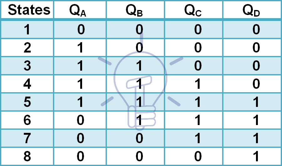
Consider a 4-bit Johnson counter with QA, QB, QC, QD as the output of 4 stages of the counter. The truth table of the 4-bit Johnson counter is given below;

4-bit Johnson counter truth table

Johnson Counter Schematic Design

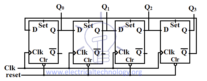
The schematic of 4-bit Johnson counter consists of 4 D-flip flops or 4 JK-flip flops. These flip-flops are connected with each other in cascade setup. The output of each flip-flop is connected with the input of the succeeding flip-flop. The complemented output of the last flip-flop is connected with the input of the first flip-flop. The Same clock input is connected with all flip-flops. There is clear input for resetting the state to default 0000. Johnson counter’s schematic design is given below.

Johnson counter schematic design

Working of Johnson Counter

The default state of Johnson counter is 0000 thus before starting the clock input we need to clear the counter using clear input.

Whenever a clock edge hits the counter the output of each flip-flop will transfer to the next stage (flip-flop) but the inverted output of the last flip-flop will shift to the first stage making the state 1000.

Upon next clock cycle, another ‘1’ will stack in from the left side as the inverted output of the last stage will be shifted to the first stage.

On next clock cycle, another ‘1’ will add in from left until the state becomes 1111.

Now that the last flip-flop’s output is ‘1’, the next clock cycle will shift the invert of the last flip-flop which is ‘0’ into the first flip-flop. It will result in stacking ‘0’ from the left side. This stacking of the first 0 will make the state 1111 into 0111.

The next coming clock cycles will stack in 0’s from the left making the states 0011, 0001 & 0000 with each clock cycle. Eventually, it reaches its default state and it starts from the beginning again.

Advantages / Disadvantages of Johnson Counter

Advantages 

  • More outputs as compared to ring counter.
  • It has same number of flip flop but it can count twice the number of states the ring counter can count.
  • It count the data in a continuous loop
  • It only needs half the number of flip-flops compared to the standard ring counter for the same MOD

Disadvantages 

  • Only 8 of the 15 states are being used.
  • It doesn’t count in a binary sequence.

Applications of Ring & Johnson Counters

Johnson counter divides a clock signal’s frequency by ‘2n’. n is the bit size of the counter. Johnson counter uses less number of flip-flops compare to a typical ring counter.

2-stage Johnson counter,also known as quadrature oscillator produce 4 outputs with 90-degree phase shift.It can easily drive a 2-phase stepper motor.

3-stage Johnson counter is used as 3-phase square wave generator having 120-degree phase shift between them.

5-stage Johnson counter is used as decade counter or decade divider.

Other applications of Johnson and Ring counters as follow:

  • Frequency counters
  • As object counters
  • Parallel to serial data conversion logic circuits
  • Analog to digital convertors.
  • Digital clocks
  • Digital triangular wave generator.
  • Generating staircase voltage
  • Frequency divider circuits of the clock signals. (Where the Input frequency divided by 2)
  • Synchronous decade counter or divider circuit
  • Timers and Rate measurement. (Time circuits, Washing machines, Alarm clock etc)
  • As a 3 phase square wave generator which produces 1200 phase shift(3 stage Johnson counter)

You may also read:

The post Ring Counter & Johnson Counter – Construction & Operation appeared first on Electrical Technology.


May 06, 2018 at 03:10AM by Department of EEE, ADBU: https://ift.tt/2AyIRVT
High Voltage Cables In a Nutshell (Technology, Bonding, Installation and Service)

Differences between the electrical characteristics of overhead transmission lines and high voltage AC cables are fundamental and must be considered. This article gives a brief introduction to cable technology, with... Read more

The post High Voltage Cables In a Nutshell (Technology, Bonding, Installation and Service) appeared first on EEP - Electrical Engineering Portal.


View more at http://electrical-engineering-portal.com/high-voltage-cables-technology
Credit- Electrical Engineering Portal. Published by Department of EEE, ADBU: tinyurl.com/eee-adbu

Digital Flip-Flops – SR, D, JK and T Flip Flops

Digital Flip-Flops – Types & Operation of Flip-Flops

What is Flip-Flop?

Digital flip-flops are memory devices used for storing binary data in sequential logic circuits. Latches are level sensitive and Flip-flops are edge sensitive. It means that the latch’s output change with a change in input levels and the flip-flop’s output only change when there is an edge of controlling signal. That control signal is known as a clock signal Q.

Types of Digital Flip-Flops

Most common types of flip-flops are as follow.

  1. SR Flip-flop
  2. D Flip-flop
  3. JK Flip-flop
  4. T Flip-flop

SR Flip-Flop

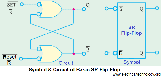
SR Flip-flop is the most basic sequential logic circuit also known as SR latch. It has two inputs known as SET and RESET. The Output “Q” is High if the input as SET is High (when the clock is triggered). If the input RESET is High when the clock is triggered, the Output “Q” would be “LOW”. Note that both the Inputs i.e. SET and RESET should not be “High” when the clock is triggered as it is considers as invalid input condition which leads to unpredictable output result.

Symbol and Circuit of Basic SR Flip-Flop

Symbol and Circuit of Basic SR Flip-Flop

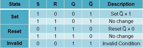
Truth Table of SR Flip-Flop

Below is the Truth table of SET-RESET Function of SR Flip-Flop.

Truth Table of SR Flip-FlopIt is clear from the truth table that

If

S =1 , R = 1, then Q and Q̅ may be logic level 1 or 0.

S =0 , R = 0, = it is invalid condition and must be avoided. The rest can be seen in the above truth table.

D Flip-Flop

D Flip-flop operation is same as D latch. The only difference is that D flip-flop changes its output only when there is an edge of the clock signal.

Truth Table

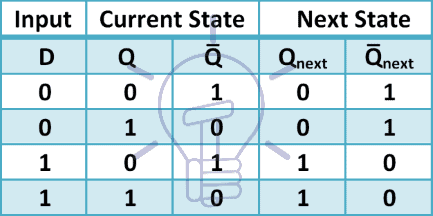
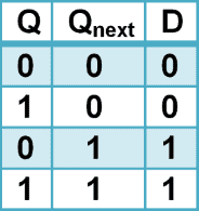
Flip-flop’s truth table consists of current and next states. It shows the output state of flip-flop after a clock cycle.

The truth table for D flip-flop is given below:

D flip-flop truth table

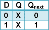
Characteristic Table

A characteristic table is a short form of the truth table. It provides the information about what the next state of the flip-flop will be on a specific input. The characteristic table of D flip-flop is given below.

characteristic table of D flip-flop

X means don’t care. It does not matter what the current state is for this input, the next state is guaranteed.

Excitation Table

Excitation table shows the necessary inputs for a current state to change into a specific next state. Excitation table of D flip-flop is given below:

Excitation table of D flip-flop

Construction of D Flip-Flop

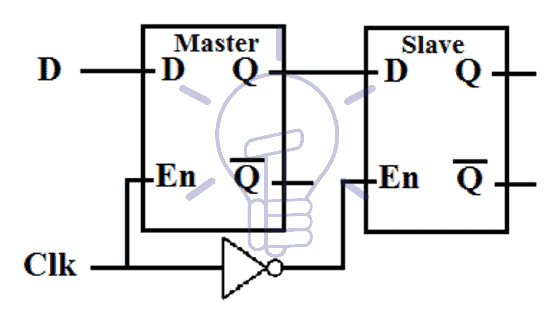
D flip-flop is made from 2 D-latches. Its schematic is given in the figure below:

schematic or Construction of D Flip-flop

The first latch is master D-latch and the second one is slave-latch. When clk = 1 the master latch will be enabled and slave latch will be disabled. The master latch will evaluate its output state as Qm = D but it will not be processed by slave latch. When clk becomes 0, the master latch will get disabled and it will not change its state and the slave latch will get enabled. The output of slave latch will get updated as Q = Qm = D. it shows that the output state only changes when the clock signal goes from 1 to 0, meaning negative or falling edge of the clock signal.

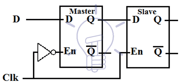
We can also design it for positive or rising edge. To change it to rising edge sensitive, we have to attach inverter with master latch’s enable pin as shown in the figure given below:

inverter with master latch%u2019s enable pin

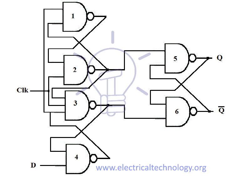
D Flip-flop can also be made using 3 S-R latches using 6 NAND gates. It is efficient as it uses less logic gate for fast speed and low cost. Its schematic is given below:

schematic of D Flip-flop made by using 3 S-R latches using 6 NAND gates

When clk = 0 , then S = 1 and R = 1, which is hold state for NAND gate SR latch. The flip-flop will hold its state.

When clk = 1 and D =1 then gate 4 output = 0 because R = 1. One input of gate 3 is low “0”, so its output = 1, which is R = 1. One input of gate 1 is low so its output = 1. That makes the output of gate 2 S = 0 because both inputs are high. R = 1, S = 0 will set the output state Q = 1.

Now if clk = 0 the S,R = 1 & the flip-flop will hold the current state.

Again when clk = 1 and D = 0. Both inputs to the gate 4 are high, so the output of gate 4 R = 0.it will reset the output state Q = 0.

Thus this flip-flop works on positive or rising edge of the clock signal.

S,R state does not go to hold state until the clock signal = 0.

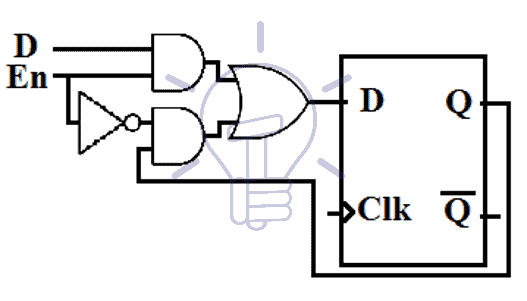
D Flip-Flop with Enable

Enable pin enables the D flip-flop to hold its last state without considering the clock signal. It does not matter if there is a clock edge, the flip-flop will hold its state if it is disabled. Its schematic is given below.

Schematic of D flip-flop with enable

When En = 0, the flip-flop will retains its state & when En = 1, it can change its state upon next clock cycle.

JK Flip-Flop

JK flip-flop is same as S-R flip-flop but without any restricted input. The restricted input of S-R latch toggles the output of JK flip-flop.

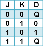
JK flip-flop is modified version of D flip-flop. We attach a combinational circuit to a D flip-flop to convert it into JK flip-flop. Its state table is given below:

Characteristic Table

A characteristic table is ashort form of the truth table. It provides the information about what the next state of the flip-flop will be on a specific input. The characteristic table of JK flip-flop is given below.

JK flip-flop characteristic table

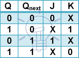
Excitation Table

Excitation table shows the necessary inputs for a current state to change into a specific next state. Excitation table of JK flip-flop is given below:

JK flip-flop Excitation table

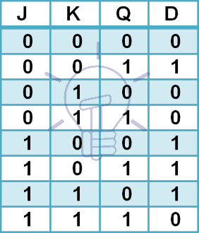
Truth Table

The truth table of JK flip-flop is given below:

JK flip-flop truth table

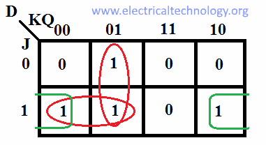
Solving the truth table using K-map, the expression for D is:

JK flip-flop K-map

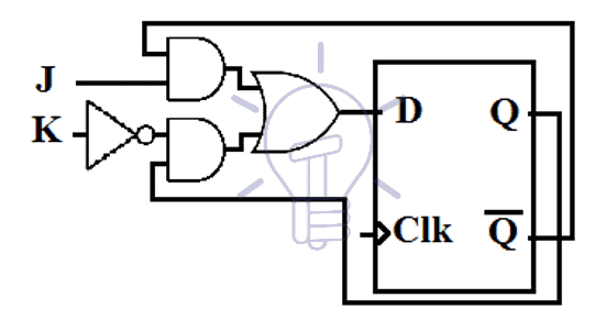
D = K̅Q + JQ̅

Its schematic is given in the figure below.

schematic JK flip-flop K-map

Symbol

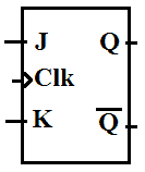
The symbol for positive or rising edge sensitive JK flip-flop is given below:

JK flip-flop symbol for positive or rising edge sensitive

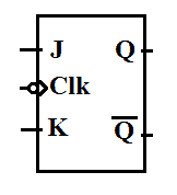
The symbol for negative or falling edge sensitive JK flip-flop is given below.

JK flip-flop symbol for negative or falling edge sensitive

JK flip-flop eliminates the problem of restricted input of SR flip-flop.

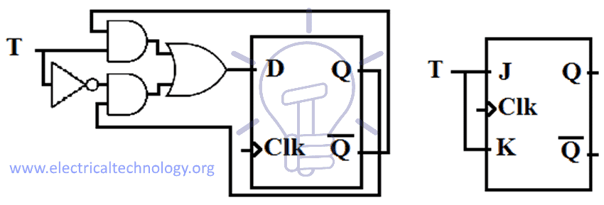
T Flip-Flop

T stands for the toggle. T flip-flop is modified version of JK flip-flop. JK inputs of JK flip-flop combine together to form a single input T. This flip-flop is called T flip-flop.

When T = 1, the output keeps changing Q = Q̅ upon each clock cycle.

When T = 0, the flip-flop hold its state Q = Q.

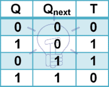
Characteristic Table

The characteristic table shows the short form of the truth table. T flip-flop characteristic table is given below:

T flip-flop characteristic table


Excitation Table

Its excitation table is given below:

T flip-flop excitation table

The schematic of T flip-flop is given below:

schematic of T flip-flop

Symbol

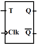
The symbol for positive or rising edge sensitive T flip-flop is given below:

T flip-flop symbol for positive or rising edge sensitive

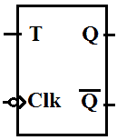
The symbol for negative or falling edge sensitive T flip-flop is given below.

T flip-flop symbol for negative or falling edge sensitive

Application of Digital Flip-Flops

Following are the common application of

  • Data storage and transfer
  • Flip-Flop synchronization
  • Serial data transfer-shift register
  • Frequency division
  • Counting
  • Event detectors

You may also read more about Digital Logic gates

Digital Logic NOT Gate – Digital Inverter Logic Gate
Digital Logic OR Gate
Digital Logic AND Gate
Exclusive-NOR (XNOR) Digital Logic Gate
Digital Logic NOR Gate
Digital Logic NAND Gate

The post Digital Flip-Flops – SR, D, JK and T Flip Flops appeared first on Electrical Technology.


May 01, 2018 at 10:33PM by Department of EEE, ADBU: https://ift.tt/2AyIRVT
Calculate Lighting Fixture’s Beam Angle and Lumen

Example 1: Calculate Lighting Fixture’s Lumen and Diameter of Illumination at surface having following details.

  • Required illumination at surface is 1390 Lux
  • The distance from Lighting Fixture to illumination surface is 3 Meter.
  • The Fixture Beam Angle is 10 Degree.

1234

Calculation:

  • Required Lux at Surface (E2) =1390 Lux.
  • Distance between Lighting Fixture and Surface (D) = 3 Meter.
  • Fixture Beam Angle (ϕ)= 10°
  • Irradiance at 1.0 meter (E1)= DxDxE2
  • Irradiance at 1.0 meter (E1)=1390x3x3 =12510 Lumen / M2
  • Irradiance at 1.0 meter (E1)= 12510 Lumen / M2
  • Solid Angle of The Lamp (Ω) =2xπx(1-COS(ϕ/2))
  • Solid Angle of The Lamp (Ω) =2×3.14x(1-COS(10/2)) =6.28x(1-0.996)
  • Solid Angle of the Lamp (Ω) =0.0239 Steradian.
  • Required Lumen of Lighting Fixtures= E1x Ω
  • Required Lumen of Lighting Fixtures=12510×0.0239
  • Required Lumen of Lighting Fixtures=299 Lumen.
  • Illumination Diameter at surface =0.018xDx ϕ
  • Illumination Diameter at surface =0.018x3x10
  • Illumination Diameter at surface =0.54 Meter.

Example 2: Calculate Lighting Fixture’s Beam Angle and Illumination Diameter at surface having following details.

  • Required illumination at surface is 22 Lux
  • Lighting Fixture Lumen is 1547 Lumen.
  • The distance from Lighting Fixture to illumination surface is 4 Meter.

Calculation:

  • Required Lux at Surface (E2) =22 Lux.
  • Distance between Lighting Fixture and Surface (D) = 4 Meter.
  • Irradiance at 1.0 meter (E1)= DxDxE2
  • Irradiance at 1.0 meter (E1)=4x4x22 =352 Lumen / M2
  • Irradiance at 1.0 meter (E1)= 352 Lumen / M2
  • Solid Angle of The Lamp (Ω) = Lumen of Lighting Fixtures / E1
  • Solid Angle of the Lamp (Ω) =1547 / 352
  • Solid Angle of the Lamp (Ω) =4.394 Steradian.
  • Solid Angle of The Lamp (Ω) =2xπx(1-COS(ϕ/2))
  • 39 =2×3.14x(1-COS(ϕ/2))
  • Fixture Beam Angle (ϕ)=145°
  • Illumination Diameter at surface =0.018xDx ϕ
  • Illumination Diameter at surface =0.018x4x145
  • Illumination Diameter at surface =10.44 Meter.

Example 3: Calculate Lux Level and Illumination Diameter at surface having following details.

  • Lighting Fixture Lumen is 299 Lumen.
  • The distance from Lighting Fixture to illumination surface is 3 Meter.
  • The Fixture Beam Angle is 10 Degree.

Calculation:

  • Required Lux at Surface (E2) =1390 Lux.
  • Distance between Lighting Fixture and Surface (D) = 3 Meter.
  • Fixture Beam Angle (ϕ)= 10°
  • Solid Angle of The Lamp (Ω) =2xπx(1-COS(ϕ/2))
  • Solid Angle of The Lamp (Ω) =2×3.14x(1-COS(10/2)) =6.28x(1-0.996)
  • Solid Angle of the Lamp (Ω) =0.0239 Steradian.
  • Lumen of Lighting Fixtures= E1x Ω
  • 299= E1x0.0239
  • Irradiance at 1.0 meter (E1)= Lumen of Lighting Fixtures / Ω
  • Irradiance at 1.0 meter (E1)=299 / 0.0239
  • Irradiance at 1.0 meter (E1)= 12506 Lumen / M2
  • Lux at Surface (E2) = E1 / (DxD)
  • Lux at Surface (E2) =12506 / (3×3)
  • Lux at Surface (E2) =1389.5 Lux
  • Illumination Diameter at surface =0.018xDx ϕ
  • Illumination Diameter at surface =0.018x3x10
  • Illumination Diameter at surface =0.54 Meter.


May 01, 2018 at 10:10PM by Department of EEE, ADBU: https://ift.tt/2AyIRVT