It offers robust performance for various applications with extensive connectivity options, and user-configurable voltage levels, making it ideal for industrial control, automation, communication, and computing fields. MYIR has introduced an embedded System-On-Module (SoM), the MYC-J7A100T, driven by the powerful Xilinx Artix-7 XC7A100T FPGA chip. This module features a high-density and speedy circuit board design, measuring […]
View more at https://www.electronicsforu.com/news/compact-high-performance-embedded-system-on-module.
Credit- EFY. Distributed by Department of EEE, ADBU: https://tinyurl.com/eee-adbu
Curated by Jesif Ahmed
High-Power Wireless EV Charging Demonstration
The future of electric vehicle charging with a 270-kW wireless power demonstration, achieving fast and efficient energy transfer. Oak Ridge National Laboratory and Volkswagen Group of America collaborated to conduct the first 270-kW wireless power transfer demonstration to a Porsche Taycan, a light-duty electric vehicle. This utilized ORNL’s polyphase wireless charging system, overcoming challenges of […]
View more at https://www.electronicsforu.com/news/high-power-wireless-ev-charging-demonstration.
Credit- EFY. Distributed by Department of EEE, ADBU: https://tinyurl.com/eee-adbu
Curated by Jesif Ahmed
View more at https://www.electronicsforu.com/news/high-power-wireless-ev-charging-demonstration.
Credit- EFY. Distributed by Department of EEE, ADBU: https://tinyurl.com/eee-adbu
Curated by Jesif Ahmed
A Code-Free 1-Coil Fan Driver
The single-coil BLDC fan driver reduces BoM costs by 25%, enhances server cooling performance, and eliminates the need for software validation. Melexis has introduced the MLX90418, an integrated 1-coil brushless DC (BLDC) fan driver. This single-coil fan driver, designed without coding, supports server-specific functions such as power-loss braking and AC power-loss management. It targets the […]
View more at https://www.electronicsforu.com/special/a-code-free-1-coil-fan-driver.
Credit- EFY. Distributed by Department of EEE, ADBU: https://tinyurl.com/eee-adbu
Curated by Jesif Ahmed
View more at https://www.electronicsforu.com/special/a-code-free-1-coil-fan-driver.
Credit- EFY. Distributed by Department of EEE, ADBU: https://tinyurl.com/eee-adbu
Curated by Jesif Ahmed
4-in-1 MEMS Air Quality Sensor For Indoors
Achieves up to 50% power savings for battery-operated devices, specifically optimized for high-condensation environments. Indoor air quality significantly impacts our health, with most people spending 90% of their time indoors, often exposed to air that is less clean than outdoor air. Poor indoor air quality can lead to respiratory diseases, allergies, heart disease, cancer, and […]
View more at https://www.electronicsforu.com/news/4-in-1-mems-air-quality-sensor-for-indoors.
Credit- EFY. Distributed by Department of EEE, ADBU: https://tinyurl.com/eee-adbu
Curated by Jesif Ahmed
View more at https://www.electronicsforu.com/news/4-in-1-mems-air-quality-sensor-for-indoors.
Credit- EFY. Distributed by Department of EEE, ADBU: https://tinyurl.com/eee-adbu
Curated by Jesif Ahmed
Introducing The TimeProvider XT Extension System For Migrating To A Modern Synchronization & Timing Systems Architecture
Critical infrastructure communication networks require highly accurate and resilient synchronization and timing, but over time these systems age out and must be migrated to a more modern architecture. Microchip Technology today announces the new TimeProvider XT Extension System, a fan-out shelf used with redundant TimeProvider 4100 grandmasters to migrate legacy BITS/SSU equipment to a modular […]
View more at https://www.electronicsforu.com/press-releases/introducing-the-timeprovider-xt-extension-system-for-migrating-to-a-modern-synchronization-timing-systems-architecture.
Credit- EFY. Distributed by Department of EEE, ADBU: https://tinyurl.com/eee-adbu
Curated by Jesif Ahmed
View more at https://www.electronicsforu.com/press-releases/introducing-the-timeprovider-xt-extension-system-for-migrating-to-a-modern-synchronization-timing-systems-architecture.
Credit- EFY. Distributed by Department of EEE, ADBU: https://tinyurl.com/eee-adbu
Curated by Jesif Ahmed
Thermal Switching Materials For High-Capacity Lithium Ion Batteries
This could be the key to safely deploying large-capacity batteries, ensuring performance and safety across various climates and operating conditions. High-capacity lithium-ion batteries (LIBs) are poised to revolutionize the electrification of vehicles and large electronics. However, to deploy these batteries on a large scale, engineers must ensure they operate safely across a range of temperatures […]
View more at https://www.electronicsforu.com/news/thermal-switching-materials-for-high-capacity-lithium-ion-batteries.
Credit- EFY. Distributed by Department of EEE, ADBU: https://tinyurl.com/eee-adbu
Curated by Jesif Ahmed
View more at https://www.electronicsforu.com/news/thermal-switching-materials-for-high-capacity-lithium-ion-batteries.
Credit- EFY. Distributed by Department of EEE, ADBU: https://tinyurl.com/eee-adbu
Curated by Jesif Ahmed
ThingPulse Pendrive S3 – A ESP32-S3 Pendrive with RGB LED, Wireless Storage and Much More
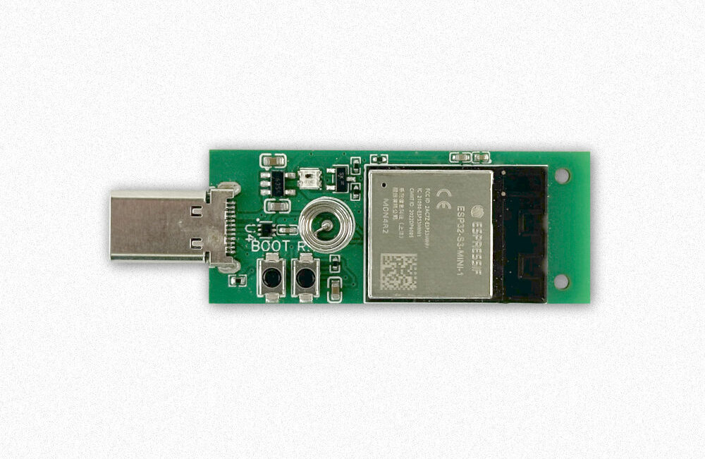
Though it’s called a Pendrive, the ThingPulse Pendrive S3 is not your average drive it’s a versatile...
The post ThingPulse Pendrive S3 – A ESP32-S3 Pendrive with RGB LED, Wireless Storage and Much More appeared first on Electronics-Lab.com.
View more at https://www.electronics-lab.com/thingpulse-pendrive-s3-a-esp32-s3-pendrive-with-rgb-led-wireless-storage-and-much-more/.
Credit- ELECTRONICS-LAB. Distributed by Department of EEE, ADBU: https://tinyurl.com/eee-adbu
Curated by Jesif Ahmed
RPGA Feather is an RP2040 and iCE40 FPGA Powered Dev Board in A Adafruit Feather From Factor
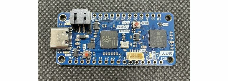
RPGA Feather by Oak Development Technologies is an RP2040 and iCE40FPGA-powered development board in an Adafruit...
The post RPGA Feather is an RP2040 and iCE40 FPGA Powered Dev Board in A Adafruit Feather From Factor appeared first on Electronics-Lab.com.
View more at https://www.electronics-lab.com/rpga-feather-is-an-rp2040-and-ice40-fpga-powered-dev-board-in-a-adafruit-feather-from-factor/.
Credit- ELECTRONICS-LAB. Distributed by Department of EEE, ADBU: https://tinyurl.com/eee-adbu
Curated by Jesif Ahmed
Standard Operating Procedures (SOPs) for GIS Substations You MUST Fully Respect
This technical article delves into the necessity of Standard Operating Procedures (SOPs) at GIS substations, emphasizing the importance of meticulous documentation, regular review, and formal approval processes to ensure that... Read more
The post Standard Operating Procedures (SOPs) for GIS Substations You MUST Fully Respect appeared first on EEP - Electrical Engineering Portal. Credit: EEP- Electrical Engineering Portal. Visit:
http://dlvr.it/T8gw0M
The post Standard Operating Procedures (SOPs) for GIS Substations You MUST Fully Respect appeared first on EEP - Electrical Engineering Portal. Credit: EEP- Electrical Engineering Portal. Visit:
http://dlvr.it/T8gw0M
Standard Operating Procedures (SOPs) for GIS Substations You MUST Fully Respect

This technical article delves into the necessity of Standard Operating Procedures (SOPs) at GIS substations, emphasizing the importance of meticulous documentation, regular review, and formal approval processes to ensure that... Read more
The post Standard Operating Procedures (SOPs) for GIS Substations You MUST Fully Respect appeared first on EEP - Electrical Engineering Portal.
View more at: https://electrical-engineering-portal.com/standard-operating-procedures-sops-gis-substations Credit- EEE - Electrical Engineering Portal. Distributed by Department of EEE, ADBU: https://tinyurl.com/eee-adbu
Curated by Jesif Ahmed.
Robot Jumps Twice Big Ben’s Height
The robot jumps 120 meters, breaking records and helping in space exploration, disaster rescue, and dangerous area surveillance. Engineers at The University of Manchester have developed a robot that can jump 120 meters, setting a new record for jumping robots. Researchers have used a combination of mathematics, computer simulations, and laboratory experiments to design a […]
View more at https://www.electronicsforu.com/news/robot-jumps-twice-big-bens-height.
Credit- EFY. Distributed by Department of EEE, ADBU: https://tinyurl.com/eee-adbu
Curated by Jesif Ahmed
View more at https://www.electronicsforu.com/news/robot-jumps-twice-big-bens-height.
Credit- EFY. Distributed by Department of EEE, ADBU: https://tinyurl.com/eee-adbu
Curated by Jesif Ahmed
Wafer-Scale 2D Material Integration With Van Der Waals Contacts
The all-stacking technique offers an efficient, high-quality, and universal approach for preparing 2D electronic devices, paving the way for future industrial-level manufacturing of these devices. In traditional fabrication processes, metal electrode deposition can damage the delicate lattices of 2D materials, degrading their electrical performance. Achieving reliable electrical contact between 2D materials and metal electrodes is […]
View more at https://www.electronicsforu.com/news/wafer-scale-2d-material-integration-with-van-der-waals-contacts.
Credit- EFY. Distributed by Department of EEE, ADBU: https://tinyurl.com/eee-adbu
Curated by Jesif Ahmed
View more at https://www.electronicsforu.com/news/wafer-scale-2d-material-integration-with-van-der-waals-contacts.
Credit- EFY. Distributed by Department of EEE, ADBU: https://tinyurl.com/eee-adbu
Curated by Jesif Ahmed
New ICeGaN GaN Power ICs Enable The Highest Efficiency Levels For Data Centres, Inverters & Industrial SMPS
Cambridge GaN Devices (CGD), the fabless, clean-tech semiconductor company that develops energy-efficient GaN-based power devices that make greener electronics possible, has launched its lowest ever on-resistance (R DS(on) ) parts which have been engineered with a new die and new packages to deliver the benefits of GaN to high-power applications such as data centres, inverters, motor drives and other industrial power supplies. New ICeGaN P2 series ICs feature R DS(on) levels down to 25 mΩ, supporting multi kW power levels with the highest efficiency.

ANDREA BRICCONI | CHIEF COMMERCIAL OFFICER, CGD
“The explosive growth of AI is leading to a significant increase in energy consumption, prompting data centre systems designers to prioritise the use of GaN for high-power, efficient power solutions. This new series of Power GaN ICs is a stepping stone for CGD to support our customers and partners by achieving and exceeding 100 kW/rack power density in data centres, required by most recent TDP (Thermal Design Power) trends for high-density computing. Turning to motor control inverters, developers are looking to GaN to reduce heat for smaller, longer-lasting system power. These are just two examples of markets that CGD is now aggressively targeting with these new high-power ICeGaN ICs. Simplified gate driver design and reduced system costs, combined with advanced high- performance packaging, make P2 series ICs an excellent choice for these applications.”
Incorporating an on-chip Miller Clamp to eliminate shoot-through losses during fast switching and implementing 0 V turn off to minimise reverse conduction losses, ICeGaN ICs outperform discrete e-Mode GaN and other incumbent technologies. The new packages offer improved thermal resistance performance as low as 0.28 K/W – again, equivalent or better than anything else currently available on the market – and the dual-gate pinout of the dual side DHDFN-9-1 (Dual Heat-spreader DFN) packagefacilitates optimal PCB layout and simple paralleling for scalability, enabling customers to address multi kW applications with ease. The new packages have also been engineered to improve productivity, with wettable flanks to simplify optical inspection.
New P2 Series ICeGaN power ICs are sampling now. The family includes four devices with R DS(on) levels of 25 mΩ and 55 mΩ, rated at 60 A and 27 A, in 10 x 10 mm footprint DHDFN-9-1 and BHDFN-9-1 (Bottom Heat-spreader DFN) packages. In common with all CGD ICeGaN products, the P2 series can be driven using any standard MOSFET or IGBT driver.
Two demo boards feature the new P2 devices: a single leg of a 3-phase automotive inverter demo board, developed in partnership with the French public R&I institute IFP Energies nouvelles, and a 3 kW totem-pole power factor correction demo board.
View more at https://www.electronicsforu.com/press-releases/new-icegan-gan-power-ics-enable-the-highest-efficiency-levels-for-data-centres-inverters-industrial-smps.
Credit- EFY. Distributed by Department of EEE, ADBU: https://tinyurl.com/eee-adbu
Curated by Jesif Ahmed
AAEON Introduces 13th Gen Intel Core Processing to the COM Express Type 10 Form Factor with its new NanoCOM-RAP
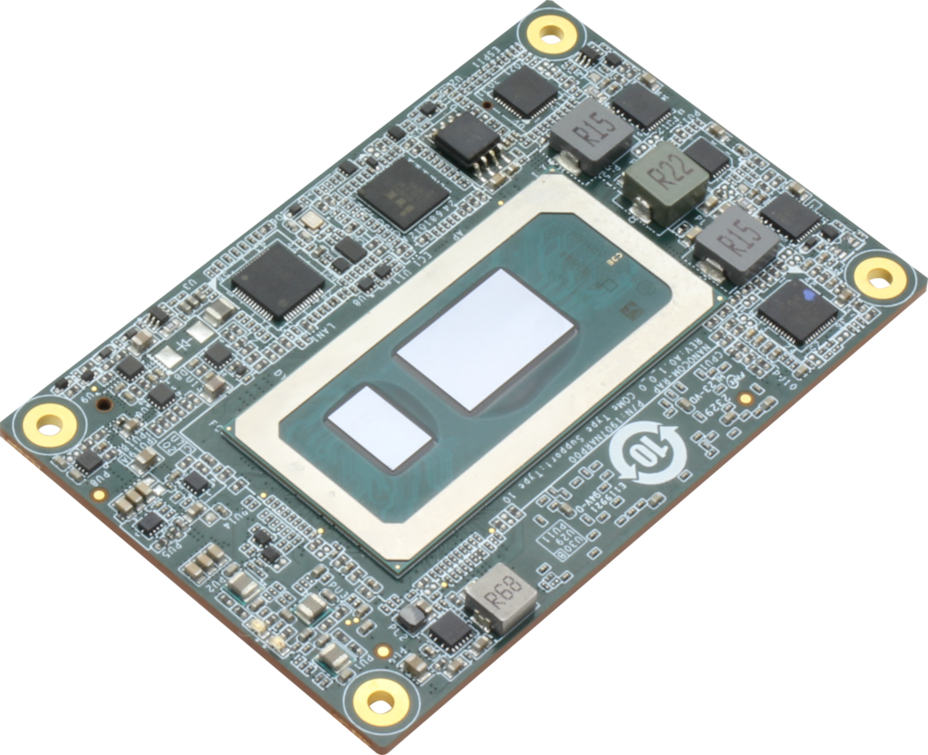
Compact, lightweight, and equipped with substantial upgrades on its predecessors, the NanoCOM-RAP represents a big step...
The post AAEON Introduces 13th Gen Intel Core Processing to the COM Express Type 10 Form Factor with its new NanoCOM-RAP appeared first on Electronics-Lab.com.
View more at https://www.electronics-lab.com/aaeon-introduces-13th-gen-intel-core-processing-to-the-com-express-type-10-form-factor-with-its-new-nanocom-rap/.
Credit- ELECTRONICS-LAB. Distributed by Department of EEE, ADBU: https://tinyurl.com/eee-adbu
Curated by Jesif Ahmed
Lynred launches ATI640, easy-to-use VGA LWIR thermal imaging module for new market players in infrared
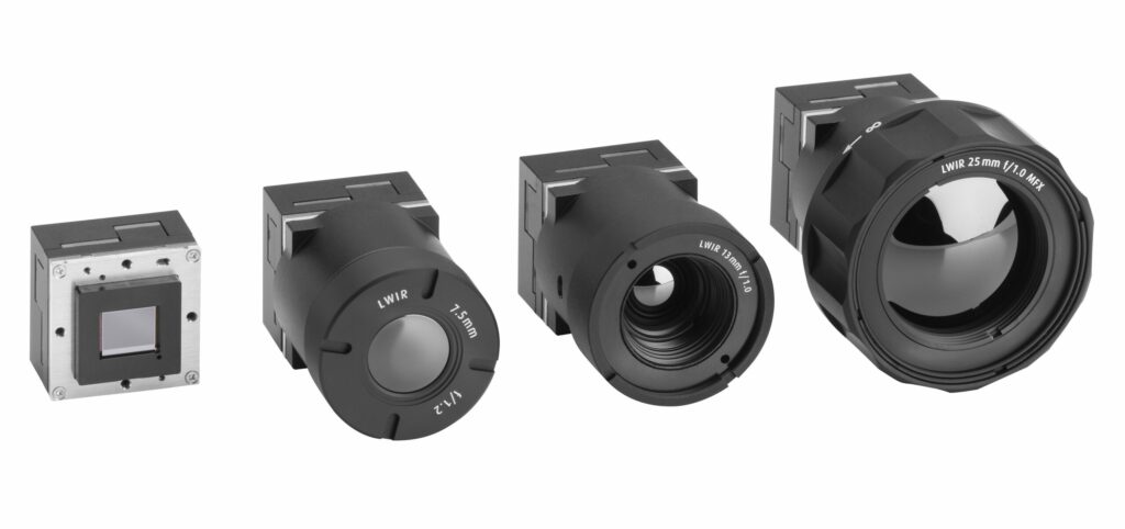
With offer of seamless IR assembly in any application, plug-and-play module makes thermal imaging more accessible...
The post Lynred launches ATI640, easy-to-use VGA LWIR thermal imaging module for new market players in infrared appeared first on Electronics-Lab.com.
View more at https://www.electronics-lab.com/lynred-launches-ati640-easy-to-use-vga-lwir-thermal-imaging-module-for-new-market-players-in-infrared/.
Credit- ELECTRONICS-LAB. Distributed by Department of EEE, ADBU: https://tinyurl.com/eee-adbu
Curated by Jesif Ahmed
TEC Driver Reference Design For 3.3V Inputs
The TEC driver reference design utilises a buck-boost converter and a microcontroller to ensure precise temperature control for sensitive applications.

Many electronic components, including laser diodes in optical modules, require precise temperature regulation to optimise performance and extend operating life. Even a slight 1°C change can cause a 0.1 nm drift in the wavelength of a laser, making temperature control down to 0.1°C critical. Thermoelectric cooling (TEC) devices, which utilise the Peltier effect, offer a solution for such precision. The direction of the current through a TEC determines whether it heats or cools. TIDA-050017, TEC driver reference design for 3.3V inputs from Texas Instruments (TI), uses a TPS63802 low quiescent current buck-boost converter in conjunction with an MSP430FR2433 microcontroller to accurately control the temperature in sensitive applications.
The applications of precise temperature control extend to various domains, including the temperature regulation of laser diodes used in optical modules, long-haul submarine communications, and metro data centre interconnects. Additionally, this technology is crucial for maintaining the optimal operating temperature of lasers and electronics packaging, ensuring their efficient and reliable performance.
The system’s features include low solution costs and a compact power stage, buck-boost converter, that occupies less than 30 mm². This power stage is also notable for its low quiescent current of just 11 μA. Additionally, the system utilises digital PI control to achieve precise temperature regulation, maintaining control within a remarkable 0.1°C. These features collectively ensure efficient and cost-effective operation.
The low quiescent current buck-boost converter is a versatile, high-efficiency, high-output current (2 A) buck-boost converter housed in a compact 3 mm × 2 mm QFN package. It efficiently handles transitions between buck, buck-boost, and boost modes without undesired toggling. In the reference design, the buck-boost converter operates off a 3.3 V regulated voltage rail. It interfaces with the TEC element between the VIN and VOUT pins, adjusting the output voltage from 1.8 V to 5 V.
The design features an integrated Power Save (PFM) mode that enhances efficiency by pausing the switching action at low-load currents. This mode is particularly beneficial when the input voltage (VI) is less than the output voltage (VO), optimising efficiency under these conditions. Conversely, when VI exceeds VO, the device employs the forced Pulse Width Modulation (PWM) mode, which involves continuous switching. This adjustment is necessary as VO may be externally charged above its target value by VI through the TEC element.
TI have tested this reference design. It comes with a bill of materials (BOM), schematics, an assembly drawing, a gerber file, etc. You can find additional data about the reference design on the company’s website. To read more about this reference design, click here.
View more at https://www.electronicsforu.com/electronics-projects/tec-driver-reference-design-for-3-3v-inputs.
Credit- EFY. Distributed by Department of EEE, ADBU: https://tinyurl.com/eee-adbu
Curated by Jesif Ahmed
Latch Vs Flip-Flop: Latch is not that BAD
The difference between latch and flip flop is that a latch is level-triggered (outputs can change as soon as the inputs change) and Flip-Flop is edge-triggered (only changes state when a control signal goes from high to low or low to high).
Latches are something in your design that always needs attention. There are tools that help designers pinpoint the existence of latches in their design as ‘must know’ information.
And then, it is the designer’s responsibility to correct if the latch usage is unintentional, as this could easily have happened due to poor RTL coding practices.
Once the latch existence is acknowledged at the synthesis level, then the downstream tools follow those conventions. This statement is suitable for ASICs, but latch existence is not acceptable for FPGAs.
It would be fine to say that FPGA tools have more accurate timing analysis for flop-based designs.
You can check the difference between FPGA and ASIC if interested.
An expert designer knows how to utilize the time-borrowing capability of a latch for slack balancing while optimizing latch-based critical paths in the design. Once he or she decides to use latches in a particular design, the engineer has to make sure that the enabled signal is stable and valid data is being captured in the latch. This helps to avoid unstable states in the design.
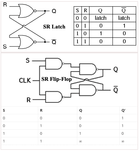
Let’s go through the latch vs flip-flop comparison and try to understand which is better than the other.
Difference between Latch and Flip Flop
| Latch | Flip-Flop |
| The latch is transparent – because the input is directly connected to the output when enable is high. It means Latch is sensitive to pulse duration (also called soft barrier) | Flip-flop is a pair of latches (master and slave flop). Flip-flop is sensitive to pulse transition. The signal only propagates through on the rising/falling edge (also called hard barrier) |
| Less Area (less gates) | More Area (more gates) because the flip-flop contains two latches. |
| Less Power (less gates) | More Power (more gates) |
| Fast – (The longer combinational path can be compensated by shorter path delays in the subsequent logic stages. That’s why, for higher performance, circuits designer are turning to latched-based design.) |
Slow – (The delay of a combinational logic path of a design using edge-triggered flip-flops is always less than the clock period except for those specified as false paths and multiple-cycle paths. Hence the longest path of a design limits the circuit performance.) |
| Require more tool manipulation and more hand calculations to verify that they meet the timing | Easy to check design timing using Static Timing Analysis (STA) tools |
| Cycle-borrowing to gain more setup time on the next register stage, as long as each loop completes in one cycleTo meet the timing in the design, Designers consider latches to adjust timing mismatch. | Data launches on one rising edge, so it must be set up before the next rising edge. If it arrives late, the system fails. If it arrives early, time is wasted due to hard edges in Flops |
| For ASICs with large clock skew, latches have substantial benefits for reducing the clock period | Even for the high-speed pulsed flip-flops with zero setup time, as they are not transparent, the impact of the clock skew is not reduced |
| Level-sensitive latches reduce the impact of the inaccuracy of wire load models and process variation. | Flip-flops demand the highly accurate wire load model and process |
| In DFT, Latches are needed as a lockup state at the clock domain crossings in the scan chain to avoid unpredictable behaviour | In DFT, use flops that can be scanned (controllable and observable) |
| In FPGA, level-sensitive transparent latches should be avoided in FPGAs | In FPGA, edge-sensitive flip-flops are used exclusively. Timings analysis is more appropriate with flops for FPGA tools |
| Circuit analysis is complex. You may see last minutes timing mismatch surprises at the implantation stage. | Circuit analysis is easy |
| High-speed microprocessor designs typically use master-slave latches instead of flip-flops so that logic can be added between the rising and falling clock edges.Most of these companies have written their own specialized STA tools to verify latch-based designs. | The most commonly used flop in the design world is D type flip-flop.FSM implementation mostly involves D Flip-flops due to a minimum number of logic gates and lesser cost as compared to other types of flip-flops. |
| For non-timing-critical configuration registers, latches work great, due to fewer gates and less power consumption | For non-power aware design, Flip flops are preferred over Latches |
| The latch is an asynchronous block. Therefore you must ensure that the combinational functions, which generate input signals for the latch, are race-free. Otherwise, they may generate glitches, which may be latched, causing hazards in your system. | A flip-flop, on the other hand, is edge-triggered and only changes state when a control signal goes from high to low or low to high |
| Latch-based design is noisy because any noise in the enable signal disrupts the latch output easily. | Flip-flop-based design is robust |
Now we can say that latch is not that bad and quietly useful in specific applications.
Comment down below what you think…
About the Author…

Arbind is a Core Competence Applications Engineer with Atrenta. He has eight years of experience in VLSI design specializing in RTL checking and optimization. Arbind has an M.Tech in VLSI Design from IP University, New Delhi. Arbind has authored many technical papers and articles on different topics for various conferences and publications. Email: arbind@atrenta.com
View more at https://www.electronicsforu.com/technology-trends/latch-not-bad-latch-vs-flip-flop.
Credit- EFY. Distributed by Department of EEE, ADBU: https://tinyurl.com/eee-adbu
Curated by Jesif Ahmed
Best practice in hard times: How to safeguard the hundreds and thousands of substations

Like it or not, hard times are in front of us, by all means. I won’t deal the hard times now, but instead, I’ll shortly say that it’s all about... Read more
The post Best practice in hard times: How to safeguard the hundreds and thousands of substations appeared first on EEP - Electrical Engineering Portal.
View more at: https://electrical-engineering-portal.com/best-practice-safeguard-substations Credit- EEE - Electrical Engineering Portal. Distributed by Department of EEE, ADBU: https://tinyurl.com/eee-adbu
Curated by Jesif Ahmed.
Best practice in hard times: How to safeguard the hundreds and thousands of substations
Like it or not, hard times are in front of us, by all means. I won’t deal the hard times now, but instead, I’ll shortly say that it’s all about... Read more
The post Best practice in hard times: How to safeguard the hundreds and thousands of substations appeared first on EEP - Electrical Engineering Portal. Credit: EEP- Electrical Engineering Portal. Visit:
http://dlvr.it/T8NJLC
The post Best practice in hard times: How to safeguard the hundreds and thousands of substations appeared first on EEP - Electrical Engineering Portal. Credit: EEP- Electrical Engineering Portal. Visit:
http://dlvr.it/T8NJLC
Remote GSM-Based Control Of Audio Hotspot Devices – A Boon Or Bane
GSM-based remote-control technology is versatile, used in audio hotspot devices and air pollution monitors. However, its misuse, such as with malicious audio blasters, raises concerns. This discussion explores the capabilities and ethical dilemmas of audio hotspot technology.
Imagine a scenario where someone is peacefully sleeping in a hotel room or unfamiliar place, only to be repeatedly disturbed by loud noises throughout the night, like the sound of a lorry unloading or an ambulance horn. These disruptions leave them feeling confused and drowsy the next morning. Initially attributing the noises to nearby traffic, they discover they were the only one hearing them. In reality, they were exposed to an audio hotspot in the room, wirelessly transmitted via a GSM modem to the hotspot hardware.
Remote control via a GSM modem is a common student project nowadays. EFY has also published articles for home control remotely using a SIM908 and Arduino board.
There have been many useful applications so far installed with such modem control in several places. noteworthy is the air pollution monitor for sensing fine particles in the air in several crowded cities. This work has been done by Prof. Tripathi and Dr Mariselvam from IIT, Kanpur . They have set up hundreds of such remote GSM-based air pollution sensing in Chennai, Delhi and several other cities.
It is shown in Fig. 1 as installed in a college premises near a crowded main street in Chennai. It actually houses a power chargeable battery, a modem, a processor and the laser-based unit for particle sensing Laser light is scattered by fine particles of 2.5 microns to 10 microns at varying angles to the ray and using photo sensors at two angles, it is able to sense the air around the laser ray and evaluate the PM2.5, PM10 values. This data, along with temperature and humidity, are sent periodically all 24 hours, and the units have been working for more than a year now. The data is collected from a central monitoring computer

There have been publications on medical monitoring applications from remote medical counsel for patients.
While such useful applications are endless, there are some malefic applications that have slowly grown in recent years. Of these the audio blaster using the audio hotspot technique is one which has caused much concern and disturbance to the authors. Like the early date pure internet data, which has today become plagued with attacks from several virus programs, every new useful development also is subject to such mischievous attempts with sadistic disturbing and stealthy ends.
What is an Audio Hotspot?
In the realm of audio technology, directional sound systems are quite literally making waves. Companies like Focusonics and Holosonics are pioneering this space, offering speakers that deliver audio in a precise, fixed direction, much like a beam of light. They can be used to send targeted audio messages to an individual in a reasonably crowded room. Imagine you are in a museum, engrossed in an artwork. A directional sound system could provide an immersive audio guide, narrating the history and significance of the piece, without disturbing other visitors.
The technology opens a world of possibilities for enhancing individual experiences in public spaces. However, every coin has two sides. These speakers are compact enough to be concealed in a mini closet or drawer. The same technology that can enrich experiences can also be weaponised for nefarious purposes. Consider a candidate in an interview room or a student in an examination hall. Targeted communication could be sent to them, compromising the integrity of the entire process.

The so-called decorative wood sheet projection on the wall houses the GSM modem and other electronic devices. A magnetometer brought near the sheet shows intense deflection, indicating the hidden electronics inside.
Audio hotspot modulates the audio signal over an ultrasound (US) frequency (of 25KHz to 40KHz). The signal is sent through an amplifier of high gain to a loudspeaker using piezoelectric elements, which can vibrate at US frequency. This outputs a sound pressure wavefront, which is narrow compared to the audio loudspeaker. Any person in the wavefront cannot ordinarily hear the US frequency because the human ear is insensitive to it. But as the beam traverses and strikes a target, the wave gets demodulated, and sound is heard. They use sounds of large intensity in these applications when they want to disturb a person
The nonlinear interaction mixes ultrasonic tones in the air to produce sum and difference frequencies. A DSB (double-sideband) amplitude-modulation scheme with an appropriately large baseband DC offset to produce the demodulating tone superimposed on the modulated audio spectrum is one way to generate the signal that encodes the desired baseband audio spectrum. This technique suffers from extremely heavy distortion as not only the demodulating tone interferes, but also all other frequencies present interfere with one another. The modulated spectrum is convolved with itself, doubling its bandwidth by the length property of the convolution. The baseband distortion in the bandwidth of the original audio spectrum is inversely proportional to the magnitude of the DC offset (demodulation tone) superimposed on the signal. A larger tone results in less distortion. F. Joseph Pompei of MIT developed technology he calls the ‘audio spotlight’ and made it commercially available in 2000 through his company Holosonics, which, according to their website, claims to have sold ‘thousands’ of their ‘audio spotlight’ systems. Disney was among the first major corporations to adopt it for use at the Epcot Center, and many other application examples are shown on the Holosonics website.]A sound signal can be aimed so that only a particular user-by, or somebody very close, can hear it. In commercial departmental stores, a transducer can be made to project a narrow beam of ultrasound modulated ultrasound that is powerful enough, at 100 to 110 dB SPL, to substantially change the speed of sound in the air that it passes through. The air within the beam behaves nonlinearly. It extracts the modulation signal from the ultrasound, resulting in sound that can be heard only along the path of the beam, or that appears to radiate from any surface that the beam strikes. (Fig3).

The trolley man can hear only the announcement particular to the compartment he is near while the other walker hears what pertains to the products, he finds near him.
Directional speakers in museums, exhibitions and art galleries can offer a huge upgrade to your visitor experience. In a quiet exhibition space, you don’t want to ruin the ambience of the environment. Visitors want to concentrate on the displays without distractions, like loudspeakers leaking sound from other exhibitions.
This technology allows a beam of sound to be projected over a long distance to be heard only in a small, well-defined area; for a listener outside the beam, the sound decreases substantially. This effect cannot be achieved with conventional loudspeakers, because sound at audible frequencies cannot be focused into such a narrow beam. In such applications, it can target sound to a single person without the peripheral sound and related noise of a loudspeaker. There are some limitations to this approach. Anything that interrupts the beam will prevent the ultrasound from propagating, like interrupting a spotlight’s beam. For this reason, most systems are mounted overhead, like lighting.
Volume: 23, Issue: 15, 01 August 2023) IEEE Sensors journal describes the circuit improvements using a sensor array. (fig 4) This enables a clearer sound than what most common devices provide. For the purpose of disturbance, a single US transducer would suffice. They generate US frequency easily using transistor circuits with an oscillator coil and amplify the signal sufficiently amplify the signal sufficiently, and then drive a 300V US transducer using a power amplifier IC. Are some people suffering as a result of increasing mass exposure of the public to ultrasound in air?

A typical circuit with a modem and an Arduino microcontroller board can use the voice recorder module APR33 to send up to sixteen loud sounds to a narrow beam. The Ultrasonic oscillator is usually a Colpitts coil-based sine wave circuit with high voltage transistors for the circuit so that the signal is at a high value of a hundred or more volts. The modulator is a diode bridge type, and it outputs the modulated signal through a high-frequency power amplifier to the piezo horn speaker

Fig. 5: A modem such as SIM 900 is used with this multiple sound blaster circuit (for disturbance or announcement or otherwise)
While there is a cacophony of discussions around the ethical implications of generative AI, technologies such as audio hotspot based directional sound and Wi-Vi (wireless vision, which lets you see through walls!) are not much discussed.
Flat builders of the huge multi-storeyed types might be hiding remote GSM-based hotspots to disturb the inmate at will for their own sadistic or other intents, even from as far away as a different country. Apparatus such as shown in the figure together with spying hardware are likely to be housed in the area shown in fig.2.
It is imperative to think about defensive measures against such technology, ensuring that one must not fear integrity compromises or the risk of continuously getting disturbed. The jammer for GSM wireless, if only permitted to use at least inside, will be a boon. Health Protection Agency (HPA) published its report, which recommended an exposure limit for the public to airborne ultrasound sound pressure levels (SPL) of 100 dB (at 25 kHz and above).
Author: K.padmanabhan, P.swaminathan And S.ananthi
View more at https://www.electronicsforu.com/technology-trends/remote-gsm-based-control-audio-hotspot-devices-boon-or-bane.
Credit- EFY. Distributed by Department of EEE, ADBU: https://tinyurl.com/eee-adbu
Curated by Jesif Ahmed
Makerfabs Agrosense_Air Review – A LoRa Powred Temperature and Humidity Sensor for Industrial and Agricultural Applications
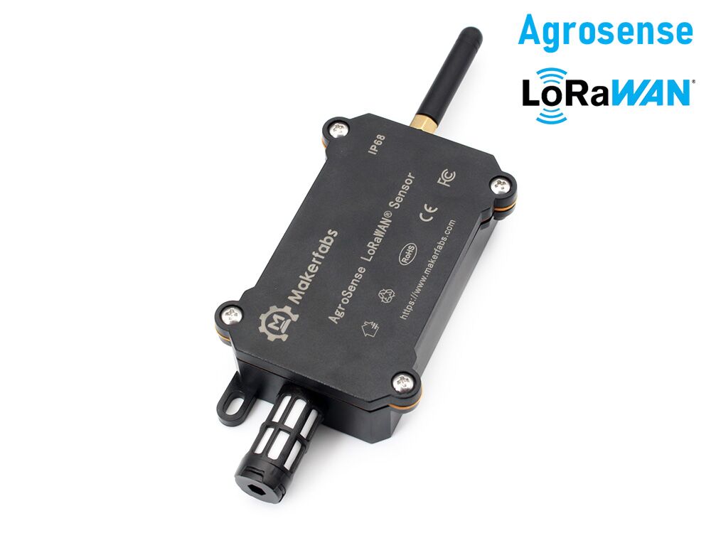
The Makerfabs Agrosense_Air is a robust LoRa-powered temperature and humidity sensor designed for use in agricultural...
The post Makerfabs Agrosense_Air Review – A LoRa Powred Temperature and Humidity Sensor for Industrial and Agricultural Applications appeared first on Electronics-Lab.com.
View more at https://www.electronics-lab.com/makerfabs-agrosense_air-review-a-lora-powred-temperature-and-humidity-sensor-for-industrial-and-agricultural-applications/.
Credit- ELECTRONICS-LAB. Distributed by Department of EEE, ADBU: https://tinyurl.com/eee-adbu
Curated by Jesif Ahmed
e-con Systems Unveils new Robust All-Weather Global Shutter Ethernet Camera for Outdoor Applications
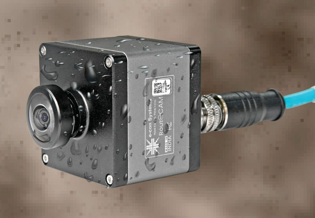
e-con Systems™, a global leader in embedded vision solutions, introduces a new Outdoor-Ready Global Shutter GigE...
The post e-con Systems Unveils new Robust All-Weather Global Shutter Ethernet Camera for Outdoor Applications appeared first on Electronics-Lab.com.
View more at https://www.electronics-lab.com/e-con-systems-unveils-new-robust-all-weather-global-shutter-ethernet-camera-for-outdoor-applications/.
Credit- ELECTRONICS-LAB. Distributed by Department of EEE, ADBU: https://tinyurl.com/eee-adbu
Curated by Jesif Ahmed
“We Aim To Boost Skills, Spark Innovation, And Fuel The Growth Of India’s Electronics Manufacturing Sector”
Everyone advises industry and academia to collaborate, but such partnerships are rare. IIT Kanpur and NMTronics have recently partnered to train professionals in electronics manufacturing. What will this lab look like? What are its goals and plans? Electronics For You’s Akanksha spoke to Prof. Nilesh Badwe, Professor-In-Charge of the NMTronics Centre of Excellence for Electronics Manufacturing and Skills Development, IIT Kanpur, and here are the key extracts from their interaction.

Q. What are this lab’s goals, and how does partnering with industry amplify its impact?
A. Bridging India’s electronics manufacturing skills gap is our mission! We focus on three core areas: delivering in-depth training for technicians, advanced training for R&D engineers, and executive training for top management. We are also pioneering research in material science for electronics, tackling issues like PCB warpage, and enabling prototype development for startups and large manufacturers. Powered by NMTronics’ CSR initiative, we aim to boost skills, spark innovation, and fuel the growth of India’s electronics manufacturing sector.
Q. Is this centre a crossroads for industry experts and students alike?
A. Our centre is a hub for industry professionals and students, dedicated to creating a collaborative space for learning and innovation. With guidance from both technical and administrative boards, we will fine-tune our curriculum and operations to cater to those eager to grow in India’s electronics manufacturing sector. Open to all, we strive to nurture a vibrant ecosystem for advancement and innovation in the field.
Q. How will industry experts be involved?
A. Industry experts will be involved in training and knowledge dissemination. These professionals will either directly teach or train designated trainers to pass on the knowledge to the students and other users. This will ensure that the curriculum remains relevant and current with industry trends and practices. We aim to bring in leading industrial experts, including those from NMTronics, Intel, material suppliers like MacDermid Alpha, and many more, to contribute to the centre’s activities.
Q. Can you share some details about this lab’s equipment?
A. Our lab will feature cutting-edge equipment essential for a fully automated SMT line, including solder paste printers, inspection systems, pick-and-place machines, reflow ovens, and automated optical inspection systems. These tools are vital for training and research in advanced electronics manufacturing processes.
Q. How will the curriculum adapt to industry needs and advancements?
A. Our flexible SMT curriculum will cater to all expertise levels, with three tiers covering basic equipment training to advanced technical skills. We shall ensure relevance by establishing a technical board for ongoing curriculum evolution based on industry feedback, providing a tailored learning experience. The programme includes theoretical, visual, and hands-on components for a comprehensive educational journey. While the training programme is in the development stage, we welcome inputs for adjustments to meet industry needs. Our training targets technicians, engineers, and high-level management, aiming to remain responsive and beneficial to all participants. This approach helps us create a comprehensive and cutting-edge curriculum.
Q. How will the centre keep up with technological advancements in the field?
A. We plan to start with state-of-the-art equipment and a flexible lab design that will adapt to tech advancements. Initially, equipment purchases will align with industry needs. We are fully aware of the dynamic nature of the electronics manufacturing industry and the ongoing advancements, such as integrating automated robots in pick-and-place (PNP) machines and including cleanroom facilities. To address this, we will design the lab in a way that allows for flexibility and scalability. Our focus is on teaching fundamental manufacturing processes, and we plan to update equipment and programmes as needed to stay relevant.
Q. How does the centre enable innovation, research, and materials development?
A. The centre will focus on advancing materials and processes for electronic manufacturing, enhancing efficiency, reliability, and sustainability. My interest in materials development for SMT applications will guide efforts to improve overall performance and environmental impact. The research will cover reflow ovens, solder paste printers, and automated inspections, focusing on developing new materials for SMT applications and exploring structure-property correlations. For example, there is a strong drive in the industry towards low-temperature solder development to enable soldering of packages with aggressive form factors, reducing carbon-dioxide emissions and power consumption.
Q. How will this centre enable electronics startups?
IIT Kanpur already has a very strong incubation ecosystem. In fact, in terms of innovation, it was ranked first last year in the NIRF Innovations rankings. We have a robust incubator called SIIC IIT Kanpur, which houses several companies focusing on electronics manufacturing. We also have one of the largest research and technology parks in India, Technopark, that houses facilities for several companies working with IIT Kanpur faculties on different R&D problems. This new centre will serve as a support system for these companies as well, providing them with access to state-of-the-art facilities and training programmes.
Q. What is NMTronics’ role, and who will maintain the lab?
A. NMTronics plays a crucial role in funding the initiative through CSR contributions. The lab is owned and managed fully by IIT Kanpur. The work is done with guidance from administrative and technical boards and industry experts. Project-based staff hired through the university will handle day-to-day maintenance, ensuring the centre’s smooth operation. Industry professionals will contribute to training and curriculum development, enhancing the lab’s effectiveness.
Q. How will the equipment procurement process work?
A. NMTronics contributes CSR funding. Equipment procurement will adhere to government norms through the Government e-Marketplace (GeM), ensuring transparency and preventing conflicts of interest. This approach allows us to source the best equipment from various suppliers.
Q. If any other firm wants to donate equipment, can they, and who should they contact?
A. Any individual or organisation interested in contributing in any manner may contact us. We welcome contributions from everyone aligned with our mission of growing and supporting the electronics manufacturing sector in India.
Q. Will there be any certification or accreditation for the programmes offered at the centre?
A. Yes, we plan to provide Joint Certification & Diploma to be issued jointly by NMTronics and IIT Kanpur for the training courses offered at the centre. This will help participants demonstrate their acquired skills and knowledge in electronics manufacturing and SMT processes. In fact, we aim to provide certified trainees with internships and potential job opportunities with industry partners, benefiting both trainees and the industry. The centre will be open to academic institutions and industry partners, offering a seamless transition from certification to internships to full-time employment.
Q. Does that mean that firms/startups outside IIT Kanpur can also get their employees trained here?
A. Yes, definitely. This centre is open for startups for building NPI along with all electronics manufacturers to use as R&D and process consultancy.
Q. What are the costs associated with enrolling for such trainings?
A. The cost of the training programs is being finalised. The pricing will be determined by the technical and administrative advisory boards. The endeavour is to establish a fair fee structure that reflects the value of the training provided.
Q. Is there a maximum capacity for training or accessing the centre at any given time?
A. We have not set a maximum capacity yet. Similar centres accommodate 25 to 50 people per batch, but our model may differ based on facility size and the nature of training. Details are still being worked out.
Q. By when will the setup be ready? And, when is the first batch expected to start?
A. Work is in progress, and the lab is expected to be fully functional by August 2024, and that is when we plan to initiate our first batch.
View more at https://www.electronicsforu.com/technology-trends/aim-to-boost-skills-spark-innovation-fuel-growth-indias-electronics-manufacturing-sector.
Credit- EFY. Distributed by Department of EEE, ADBU: https://tinyurl.com/eee-adbu
Curated by Jesif Ahmed
PCB Testing With High Speed And Accuracy
The flying probe test system speeds up and economizes testing for prototypes and small batches, enhancing fault diagnosis and repair.

The GRS550 flying probe test system, presented by Polar Instruments GmbH, advances from its forerunner, the GRS500, which is known for setting benchmarks in the electronics industry with its economical and user-friendly features. The new model showcases improved drive technology, which enhances test speeds and positioning accuracy, as per the manufacturer’s claims. Particularly effective in situations where adapter-based testing proves uneconomical, the GRS550 utilizes nodal impedance analysis and high-resolution imaging to compare a standard PCB with the one tested, facilitating effective fault diagnosis.
This system is tailored for prototype development, new product introductions, and small-batch production, where conventional in-circuit tests or multi-pin flying probers would incur high costs. It capitalizes on extensive CAD data and sophisticated fault diagnosis technologies to deliver comprehensive testing capabilities. With minimal setup time and lower costs, the system is designed for ease of use, allowing quick results without intricate programming. Its capability for rapid fault localization makes it a valuable tool in accelerating repairs of PCB assemblies and reducing the time to market for prototypes.
Equipped to manage all types of component technologies, the test system features a maximum fly height of 100 mm and dual live video cameras, ensuring a thorough fault analysis across SMT, PTH, and BGA components. This robust configuration enables precise and cost-effective troubleshooting, providing detailed coverage and reliability in fault detection across various PCB assemblies.
“This allows operators to easily generate important test results without having to carry out complex programming on fully automated systems, which are also usually oversized for these requirements,” says Reischer. “Fault analysis on complex electronic assemblies is not an easy task,” continues Reischer, adding: “The GRS550 was developed for rapid fault localization and thus enables fast and efficient repair of PCB assemblies. This saves the customer time and money and can reduce time-to-market, especially in prototype manufacturing.”
View more at https://www.electronicsforu.com/news/pcb-testing-with-high-speed-and-accuracy.
Credit- EFY. Distributed by Department of EEE, ADBU: https://tinyurl.com/eee-adbu
Curated by Jesif Ahmed
Can Large Language Models Help Robots To Navigate?
MIT and MIT-IBM Watson AI Lab researchers have created a navigation method that converts visual inputs into text to guide robots through tasks using a language model.

Credits:Credit: iStock
Someday, you might want a home robot to carry laundry to the basement, a task requiring it to combine verbal instructions with visual cues. However, this is challenging for AI agents as current systems need multiple complex machine-learning models and extensive visual data, which are hard to obtain.
Researchers from MIT and the MIT-IBM Watson AI Lab have developed a navigation method that translates visual inputs into text descriptions. A large language model then processes these descriptions to guide a robot through multistep tasks. This approach, which uses text captions instead of computationally intensive visual representations, allows the model to generate extensive synthetic training data efficiently.
Solving a vision problem with language
Researchers have developed a navigation method for robots using a simple captioning model that translates visual observations into text descriptions. These descriptions, along with verbal instructions, are input into a large language model, which then decides the robot’s next step. After each step, the model generates a scene caption to help update the robot’s trajectory, continually guiding it towards its goal. The information is standardized in templates, presenting it as a series of choices based on the surroundings, like choosing to move towards a door or an office, streamlining the decision-making process.
Advantages of language
When tested, this language-based navigation approach didn’t outperform vision-based methods but offered distinct advantages. It uses fewer resources, allowing for rapid synthetic data generation—for instance, creating 10,000 synthetic trajectories from only 10 real-world ones. Also, its use of natural language makes the system more understandable to humans and versatile across different tasks, using a single type of input. However, it does lose some information that vision-based models capture, like depth. Surprisingly, combining this language-based approach with vision-based methods improves navigation capabilities.
Researchers aim to enhance their method by developing a navigation-focused captioner and exploring how large language models can demonstrate spatial awareness to improve navigation.
View more at https://www.electronicsforu.com/news/can-large-language-models-help-robots-to-navigate.
Credit- EFY. Distributed by Department of EEE, ADBU: https://tinyurl.com/eee-adbu
Curated by Jesif Ahmed
Industry’s Leading Pre-Driver For 5G mMIMO Systems
It exemplifies the company’s innovative approach to enhancing 5G infrastructure, providing customers with advanced solutions for efficient and scalable deployment.

Qorvo has unveiled the QPA9822, the industry’s highest gain pre-driver. This component offers 39dB gain at 3.5 GHz and achieves a peak power of +29dBm, demonstrating the company’s commitment to advancing 5G technology and solidifying its leadership in cellular infrastructure.
The key features are:
- Housed in a compact 16-pin, 3 x 3 mm SMT package
- Footprint and pin-compatible with the QPA9122M high-gain and high-linearity driver amplifier
The QPA9822 is a wideband, high-gain, high-linearity driver amplifier designed specifically for 32-node massive MIMO (mMIMO) systems. It supports wideband 5G New Radio (NR) instantaneous signal bandwidths of up to 530 MHz, making it ideal for the N77 band, which is critical for 5G deployment and other mMIMO applications. It not only delivers the highest gain available on the market for 5G pre-drivers today but also provides a scalable solution for 32T and 64T radios. This helps ensure ease of deployment in popular bands across all geographies for 5G mMIMO systems.
The driver is internally matched to 50 ohms (Ω) across its operating frequency band of 3.3 – 4.2 GHz and features a fast enable/disable function through the VEN pin. It also offers external bias control for linearity optimization, supporting up to 530 MHz of instantaneous bandwidth. This compatibility allows for easy integration into both existing and new designs, reducing time-to-market for customers.
View more at https://www.electronicsforu.com/news/industrys-leading-pre-driver-for-5g-mmimo-systems.
Credit- EFY. Distributed by Department of EEE, ADBU: https://tinyurl.com/eee-adbu
Curated by Jesif Ahmed
JOB: Lead Electronics Engineer – Industrial IOT At Siemens In Bengaluru
APPLY HERE
Location: Bengaluru
Company: Siemens
You’ll Break New Ground By
- Responsible for the design and development of electronic products till the handover of the design into production covering several stages of development cycle.
- Analyze technical requirements of projects and be a “hands on technologist”, i.e., translate system level specifications into working circuits and prototypes.
- Responsible for all levels of interaction with customers, project management and time-line adherence.
You’re excited to build on your existing expertise:
- With a Bachelor’s/master’s degree in electronics or related discipline with 3-20 years of relevant experience in complex electronics design
- Should be passionate about electronics and have a strong proactive drive to provide solutions.
- Should have an entrepreneurial drive to make things work and take end to end responsibilities.
- Should be unassuming and attack problems from fundamentals putting extra effort where needed.
- Should be able to execute multiple roles (design, handling customers, managing projects etc.…)
- Strong experience in analog and digital circuit design, making design decisions, debugging.
- Should have very good understanding of all common electronic elements –
- For example, data converters, bus protocols, signal conditioning, operational amplifier, Power-supply topologies etc.
- Strong understanding of electronic circuit design concepts using discrete electronic components – For example, BJTs, FETs, Diodes (Schottky, Zener…) etc.….
- Strong competence in simulation of circuits with tools like LTSpice
- Good experience in taking a concept from design to production through all stages.
- Should be able to provide solutions considering a holistic system design that includes software, PCB, mechanical, thermal, manufacturability.
- Proficiency in microprocessor/controller architectures and some coding experience is preferable.
- Should have experience in leading small project groups (3-7 people)
- Strong understanding of design for electromagnetic compatibility
- Exposure to ISO61508 / ISO 26262 and electronic design concepts (de-rating, up-rating) is a plus
- Experience in designing battery operated systems, understanding of Energy Harvesting circuits, protocols like BLE/WiFi/NBIoT etc. would be wonderful.
View more at https://www.electronicsforu.com/career/job-lead-electronics-engineer-industrial-iot-at-siemens-in-bengaluru.
Credit- EFY. Distributed by Department of EEE, ADBU: https://tinyurl.com/eee-adbu
Curated by Jesif Ahmed
JOB: Hardware Engineer At Enphase Energy In Bengaluru
APPLY HERE
Location: Bengaluru
Company: Enphase Energy
What you will be doing
- Develop new products and variants through the product lifecycle.
- Work in cross-functional teams of hardware, firmware, test automation and mechanical engineers.
- Specify, design, verify and debug complex circuits for our inverters.
- Performance test products and sub-systems
- Design support for cost reduction proposals, Failure root-cause analysis and alternative part qualification.
- Assist product compliance engineers to achieve global certifications for our products.
- Specify engineering requirements, create test plans, and generate test reports.
- Provide technical mentoring to manufacturing and field application engineers.
- Mentor junior engineers and supervise lab work.
- Raise the bar for technical excellence, accurate documentation, and scientific rigor.
- Provide subject matter expertise at an advanced level.
Who you are and what you bring
- B.E. and 4+ years’ experience outside of university or
- Masters and 2+ years.
- Developing electronic products from the concept stage to market launch in a commercial environment.
- Extensive knowledge of circuit schematic, PCB layout and simulation tools
- Practical experience of in-depth bench testing, V&V testing, and debugging of hardware designs.
- Strong Trouble-shooting and problem solving skillset.
- Some experience of using Python, Embedded software development, and working in a Test Automation environment.
- Power Electronics circuits
- End to end electronics design development for high-volume manufacturing
- End to end electronics design development in regulated industry.
- Power supply and inverter topologies
- Field Quality Improvement and Cost reduction through VAVE.
View more at https://www.electronicsforu.com/career/hardware-engineer-enphase-energy-bengaluru.
Credit- EFY. Distributed by Department of EEE, ADBU: https://tinyurl.com/eee-adbu
Curated by Jesif Ahmed
JOB: Power Electronics Hardware Engineer At Su-vastika Systems Private Limited In Gurugram
APPLY HERE ON LINKEDIN
Location: Gurugram
Company: Su-vastika Systems Private Limited
Company Description
Su-vastika Systems Private Limited is a leading power backup solutions company located in Gurugram. Our mission is to provide efficient, cost-effective, and environmentally friendly continuous power supply solutions. With a foundation of innovation, our advanced products cater to a wide range of customers, including UPS, batteries, and solar solutions. Backed by the expertise of Mr. Kunwer Sachdev, the Solar Man of India, who founded Su-Kam Power Systems, Su-vastika is committed to delivering cutting-edge power solutions.
Role Description
This is a full-time hybrid role for a Power Electronics Hardware Engineer at Su-vastika Systems Private Limited. The engineer will be responsible for hardware development, circuit design, and electronics hardware design. They will be involved in designing and testing various power electronics hardware components. While this role is primarily located in Gurugram, there is flexibility for some remote work.
Qualifications
- Hardware Development and Electronics Hardware Design skills
- Expertise in Circuit Design
- Knowledge of Computer Hardware
- Experience in power electronics hardware design
- Strong problem-solving and troubleshooting abilities
- Excellent communication and teamwork skills
- Bachelor’s or Master’s degree in Electrical or Electronics Engineering
View more at https://www.electronicsforu.com/news/power-electronics-hardware-engineer-su-vastika-systems.
Credit- EFY. Distributed by Department of EEE, ADBU: https://tinyurl.com/eee-adbu
Curated by Jesif Ahmed
7805 Voltage Regulator IC Pinout, Circuit, and Applications
Voltage sources in a circuit may have fluctuations resulting in not providing fixed voltage outputs. A voltage regulator IC maintains the output voltage at a constant value. 7805 Voltage Regulator, a member of the 78xx series of fixed linear voltage regulators used to maintain such fluctuations, is a popular voltage regulator integrated circuit (IC).
The xx in 78xx indicates the output voltage it provides. 7805 IC provides +5 volts regulated power supply with provisions to add a heat sink.
7805 Voltage Regulator IC Specifications
- Minimum Input voltage is 7V
- Maximum Input Voltage is 35V
- Current rating Ic = 1A
- Maximum Output Voltage VMax=5.2V
- Minimum Output Voltage VMin=4.8V
LM7805 Voltage Regulator Pinout
Below you can see the 7805 Voltage Regulator Pin Diagram.
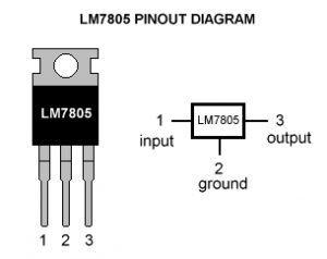
| Pin No. | Pin | Function | Description |
| 1 | INPUT | Input voltage (7V-35V) | In this pin of the IC positive unregulated voltage is given in the regulation. |
| 2 | GROUND | Ground (0V) | In this pin where the ground is given. This pin is neutral for equally the input and output. |
| 3 | OUTPUT | Regulated output; 5V (4.8V-5.2V) | The output of the regulated 5V is taken out at this pin of the IC regulator. |
As you may have noticed, there is a significant difference between the input voltage & the output voltage of the voltage regulator. This difference between the input and output voltage is released as heat. The greater the difference between the input and output voltage, more the heat is generated.
If the regulator does not have a heat sink to dissipate this heat, it can get destroyed and malfunction. Hence, it is advisable to limit the voltage to a maximum of 2-3 volts above the output voltage.
So, we now have 2 options. Either design your circuit so that the input voltage going into the regulator is limited to 2-3 volts above the output regulated voltage or place an appropriate heatsink, that can efficiently dissipate heat.
7805 IC Heating Problem
7805 voltage regulator is not very efficient and has drop-out voltage problems. A lot of energy is wasted in the form of heat. If you are going to be using a heatsink, better calculate the heatsink size properly. The below formula should help in determining the appropriate heatsink size for such applications.
Heat generated = (input voltage – 5) x output current
If we have a system with an input of 15 volts and the output current required is .5 amperes,
Then we have: (15 – 5) x 0.5 = 10×0.5 = 5W;
5W energy is being wasted as heat, hence an appropriate heatsink is required to disperse this heat. On the other hand, the energy actually being used is: (5 x 0.5Amp) = 2.5W.
So twice the energy, that is actually utilized is wasted. On the other hand, if 9V is given as input at the same amount of load: (9-5) x 0.5 = 2W
2W energy will be wasted as heat.
What should we do then?
Remember… higher the input voltage, the less efficient your IC7805 will be.
An estimated efficient input voltage would be about 7.5V.
Why do we use Capacitors with 7805?
If your voltage regulator is situated more than 25cm (10 inches) from the power supply, capacitors are needed to filter residual AC noise. Voltage regulators work efficiently on a clean DC signal being fed. The bypass capacitors help reduce AC ripple.
Essentially, they short AC noise from the voltage signal and allow only DC voltage into the regulator. The two capacitors are not necessarily required and can be omitted if you are not concerned about line noise.
However, for a mobile phone charger or logic assessment, you require a nice clean DC line. Capacitors will be beneficial in this case as they are good at maximizing voltage regulation. The values of capacitors can also be changed slightly.
You can check Why Are Filter Capacitors Used in Some Battery Charger Circuits?
Let’s take a look at what makes the IC tick.
Voltage Regulator 7805 IC Circuit
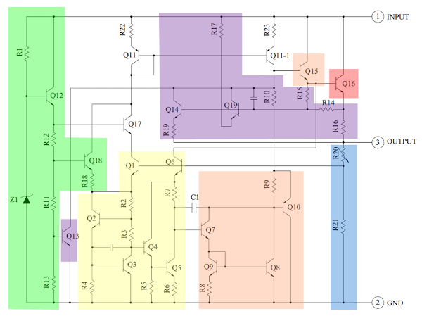
The heart of the 7805 IC is a transistor (Q16) that controls the current between the input and output and thus controls the output voltage. The bandgap reference (yellow) keeps the voltage stable.
It takes the scaled output voltage as input (Q1 and Q6) and provides an error signal (to Q7) for indication if the voltage is too high or low.
The key task of the bandgap is to provide a stable and accurate reference, even as the chip’s temperature changes.
The error signal from the bandgap reference is amplified by the error amplifier (orange). This amplified signal controls the output transistor through Q15. This closes the negative feedback loop controlling the output voltage.
The startup circuit (green) provides initial current to the bandgap circuit, so it doesn’t get stuck in an “off” state. The circuit in purple provides protection against overheating (Q13), excessive input voltage (Q19), and excessive output current (Q14).
These circuits reduce the output current or shut down the regulator, protecting it from damage in case of a fault. The voltage divider (blue) scales down the voltage on the output pin for use by the bandgap reference.
Scaling the Output
The 7805’s scaled output provides the input voltage (Vin) to the bandgap reference and the bandgap provides an error signal as the output. The 7805’s bandgap circuit removes the feedback loop that exists inside a traditional bandgap reference. Instead, the entire chip becomes the feedback loop.
If the output voltage is correct (5V), then the voltage divider provides 3.75V at Vin. Any change in output voltage propagates through Q6 and R7, causing the voltage at the base of Q7 to rise or fall accordingly.
This change is amplified by Q7 and Q8, generating the error output. The error output, in turn, decreases or increases the current through the output transistor. The negative feedback loop adjusts the output voltage until it is correct.
IC 7805 Voltage Regulator Applications
7805 IC is used in a wide range of circuits. The major ones are:
- Fixed-Output Regulator
- Positive voltage Regulator in Negative voltage Configuration
- Adjustable Output Regulator
- Current Regulator
- Adjustable DC Voltage Regulator
- Regulated Dual-Supply
- Output Polarity-Reversal-Protection Circuit
- Reverse bias projection Circuit
7805 Voltage regulator also finds usage in building circuits for inductance meters, phone chargers, portable CD player, infrared remote-control extension, and UPS power supply circuits. Also, we designed a Stopwatch Circuit using IC7805.
The slideshow below also highlights some points with voltage regulators.
Credit: niiraz
Complete technical detailed information about the 7805-voltage regulator IC can be found in the 7805 IC datasheet.
What does a 7805 voltage regulator do?
A 7805 voltage regulator is an integrated circuit designed to maintain a constant output voltage despite changes in input voltage and load. Specifically, the 7805 is a positive voltage regulator that ensures a stable +5V output, making it a popular choice for powering various electronic components and circuits.
How much voltage can 7805 handle?
The 7805 voltage regulator is typically used to provide a fixed +5V output. To ensure proper operation, the input voltage should be higher than the desired output voltage plus a small overhead voltage for the regulator to function correctly. Generally, the input voltage can range from around 7V to 35V, allowing the 7805 to handle a wide range of input voltages while maintaining a steady +5V output.
What temperature should a 7805 voltage regulator be?
The operating temperature of a 7805 voltage regulator is typically specified by its manufacturer. Standard operating temperature ranges are often from 0°C to 125°C. However, variations exist, and some models might have extended temperature ranges to accommodate specific applications.
What is the difference between LM7805 and 7805?
The terms “LM7805” and “7805” both refer to the same type of voltage regulator. The LM prefix indicates that the component is manufactured by National Semiconductor (now a part of Texas Instruments), and it’s often included for clarity. So, the LM7805 and 7805 both represent the same voltage regulator with a fixed +5V output.
View more at https://www.electronicsforu.com/technology-trends/learn-electronics/7805-ic-voltage-regulator.
Credit- EFY. Distributed by Department of EEE, ADBU: https://tinyurl.com/eee-adbu
Curated by Jesif Ahmed
Rohde & Schwarz presents R&S RT-ZISO isolated probing system for precise measurements of fast switching signals
Rohde & Schwarz has developed the R&S RT-ZISO isolated probing system, further elevating its cutting-edge oscilloscope...
The post Rohde & Schwarz presents R&S RT-ZISO isolated probing system for precise measurements of fast switching signals appeared first on Electronics-Lab.com.
View more at https://www.electronics-lab.com/rohde-schwarz-presents-rs-rt-ziso-isolated-probing-system-for-precise-measurements-of-fast-switching-signals/.
Credit- ELECTRONICS-LAB. Distributed by Department of EEE, ADBU: https://tinyurl.com/eee-adbu
Curated by Jesif Ahmed
Subscribe to:
Comments (Atom)