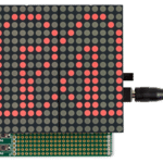
 Why do LED displays still feel limited? A design approach removes size, wiring, and power limits, helping engineers build displays faster. Design engineers often face challenges when trying to display information on LED matrices. Small 8×8 LED arrays are widely used, but they come with significant limitations. Characters and symbols are constrained by the size […]
View more at https://www.electronicsforu.com/electronics-projects/display-driver-shield-reference-design.
Credit- EFY. Distributed by Department of EEE, ADBU: https://tinyurl.com/eee-adbu
Curated by Jesif Ahmed
 Hard to use PLCs and control machines? These displays make operation clear, show information, connect with controllers, and let factories set up custom screens fast. Industrial manufacturing is becoming more complex as processes rely on networked systems and real-time data. Programmable logic controllers (PLCs), once simple logic units, are now evolving into connected computing nodes […]
 Automotive OEMs gain flexible, high-performance touchscreen solutions for evolving cockpit interfaces, supporting accuracy, uniformity, and immersive user experiences. Automotive displays are continuing to grow in size and complexity as cockpit interfaces are becoming more immersive and software-defined. OEMs are pushing the boundaries of display size, shape, and technology, creating a need for touchscreen controllers that […]
 India’s first AI defined two wheeler platform shifts vehicle intelligence from software updates to real time control of energy and materials. As electric two wheelers integrate higher levels of electronics, software, and connectivity, manufacturers face rising complexity in managing performance, energy efficiency, thermal behaviour, and lifecycle reliability. Existing mechanically and software defined architectures limit how […]
 To execute large-scale synchronised flights involving over 1000 drones, India’s first drone swarm was developed as early as 2018. How has the journey been ever since? What is the future? Sarita Ahlawat from Botlab Dynamics, the firm behind this innovation, narrates their story to EFY’s Nitisha Dubey. Q. What did the company focus on during […]
 In this video, we explore a DIY proof-of-concept project called “Musical Temperature Alarm”, published on Electronics For You.When the temperature rises (for example, by bringing a hot soldering iron close), the circuit detects it. Once the set limit is crossed, the music starts playing.In this video, we explore a DIY proof-of-concept project called “Musical Temperature […]
 Ice on aircraft, drones, and turbines can cause crashes and delays. A sensor spots ice instantly and could change how we handle it. Ice on aircraft, drones, and wind turbines causes serious problems. It can damage vehicles, increase maintenance costs, ground operations, delay flights, and even lead to crashes. For drones, even a thin line […]
 APPLY HERE Location: Chennai Company: Aptiv Your Role Your Background Key ingredients for succeeding in this role are your:
 By stacking active devices above existing circuitry, the platform reduces data transfer energy while increasing integration density and performance. Growing computational workloads are increasing energy losses caused by constant data transfer between logic and memory in conventional microelectronic architectures. As device scaling slows, reducing interconnect energy and improving integration density have become critical for sustaining […]